参数资料
| 型号: | AD795JR-REEL7 |
| 厂商: | Analog Devices Inc |
| 文件页数: | 8/20页 |
| 文件大小: | 0K |
| 描述: | IC OPAMP JFET 1.6MHZ LN 8SOIC |
| 标准包装: | 1,000 |
| 放大器类型: | J-FET |
| 电路数: | 1 |
| 转换速率: | 1 V/µs |
| -3db带宽: | 1.6MHz |
| 电流 - 输入偏压: | 1pA |
| 电压 - 输入偏移: | 100µV |
| 电流 - 电源: | 1.3mA |
| 电流 - 输出 / 通道: | 10mA |
| 电压 - 电源,单路/双路(±): | 8 V ~ 36 V,±4 V ~ 18 V |
| 工作温度: | 0°C ~ 70°C |
| 安装类型: | 表面贴装 |
| 封装/外壳: | 8-SOIC(0.154",3.90mm 宽) |
| 供应商设备封装: | 8-SO |
| 包装: | 带卷 (TR) |
AD795
Rev. C | Page 16 of 20
PREAMPLIFIER APPLICATIONS
The low input current and offset voltage levels of the AD795
together with its low voltage noise make this amplifier an
excellent choice for preamplifiers used in sensitive photodiode
applications. In a typical preamp circuit, shown in Figure 45,
the output of the amplifier is equal to:
VOUT = ID (Rf) = Rp (P) Rf
where:
ID is the photodiode signal current, in amps (A).
Rp is the photodiode sensitivity, in amps/watt (A/W).
Rf is the value of the feedback resistor, in ohms (Ω).
P is the light power incident to photodiode surface, in watts (W).
An equivalent model for a photodiode and its dc error sources
butes an output voltage error, which is proportional to the value
of the feedback resistor. The offset voltage error, VOS, causes a
dark current error due to the photodiode’s finite shunt resistance,
Rd. The resulting output voltage error, VE, is equal to:
VE = (1 + Rf/Rd) VOS + Rf IB
A shunt resistance on the order of 109 Ω is typical for a small
photodiode. Resistance Rd is a junction resistance, which
typically drops by a factor of two for every 10°C rise in
temperature. In the AD795, both the offset voltage and drift are
low, which helps minimize these errors.
RD
ID
IB
CD
50pF
CF
10pF
VOS
RF
1G
PHOTODIODE
OUTPUT
00
845
-04
6
Figure 46. A Photodiode Model Showing DC Error Sources
MINIMIZING NOISE CONTRIBUTIONS
The noise level limits the resolution obtainable from any
preamplifier. The total output voltage noise divided by the
feedback resistance of the op amp defines the minimum
detectable signal current. The minimum detectable current
divided by the photodiode sensitivity is the minimum
detectable light power.
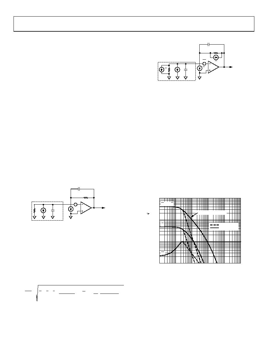
Sources of noise in a typical preamp are shown in Figure 47.
The total noise contribution is defined as:
2
1
Rf
Cf
s
Rd
Cd
s
Rd
Rf
en
Rf
Cf
s
Rf
is
if
in
V
OUT
RD
IS
CD
50pF
CF
10pF
RF
1G
PHOTODIODE
OUTPUT
00
84
5-
0
4
7
en
IN
IF
IS
Figure 47. Noise Contributions of Various Sources
Figure 48, a spectral density vs. frequency plot of each source’s
noise contribution, shows that the bandwidth of the amplifier’s
input voltage noise contribution is much greater than its signal
bandwidth. In addition, capacitance at the summing junction
results in a peaking of noise gain in this configuration. This
effect can be substantial when large photodiodes with large shunt
capacitances are used. Capacitor Cf sets the signal bandwidth
and limits the peak in the noise gain. Each source’s rms or root-
sum-square contribution to noise is obtained by integrating the
sum of the squares of all the noise sources and then by
obtaining the square root of this sum. Minimizing the total area
under these curves optimizes the preamplifier’s overall noise
performance.
An output filter with a passband close to that of the signal can
greatly improve the preamplifier’s signal to noise ratio. The
photodiode preamplifier shown in Figure 47, without a bandpass
filter, has a total output noise of 50 μV rms. Using a 26 Hz
single-pole output filter, the total output noise drops to 23 μV
rms, a factor of 2 improvement with no loss in signal bandwidth.
10V
1V
100nV
10nV
1
10
100
1k
10k
100k
FREQUENCY (Hz)
O
UT
P
UT
V
O
L
T
AG
E
NO
IS
E
(
V
/
Hz
)
00
84
5-
0
4
8
SIGNAL BANDWIDTH
WITH FILTER
NO FILTER
en
IN
IQ AND IF
Figure 48. Voltage Noise Spectral Density of the Circuit of Figure 47 With and
Without an Output Filter
相关PDF资料 |
PDF描述 |
|---|---|
| MAX4257ESA+ | IC OP AMP R-R LN 8-SOIC |
| BK1/GMA-6-R | FUSE 6A 125V FAST GLASS 5X20 UL |
| TSM-105-01-T-SV-P-TR | CONN HEADER 5POS .100" SNGL SMD |
| MAX4292EUA+ | IC OP AMP R-R I/O 8-UMAX |
| 2027-47-BT1LF | GAS DISCHARGE TUBE |
相关代理商/技术参数 |
参数描述 |
|---|---|
| AD795JRZ | 功能描述:IC OPAMP JFET 1.6MHZ LN 8SOIC RoHS:是 类别:集成电路 (IC) >> Linear - Amplifiers - Instrumentation 系列:- 标准包装:2,500 系列:- 放大器类型:通用 电路数:4 输出类型:- 转换速率:0.6 V/µs 增益带宽积:1MHz -3db带宽:- 电流 - 输入偏压:45nA 电压 - 输入偏移:2000µV 电流 - 电源:1.4mA 电流 - 输出 / 通道:40mA 电压 - 电源,单路/双路(±):3 V ~ 32 V,±1.5 V ~ 16 V 工作温度:0°C ~ 70°C 安装类型:表面贴装 封装/外壳:14-TSSOP(0.173",4.40mm 宽) 供应商设备封装:14-TSSOP 包装:带卷 (TR) 其它名称:LM324ADTBR2G-NDLM324ADTBR2GOSTR |
| AD795JRZ-REEL | 功能描述:IC OPAMP JFET 1.6MHZ LN 8SOIC RoHS:是 类别:集成电路 (IC) >> Linear - Amplifiers - Instrumentation 系列:- 标准包装:1 系列:- 放大器类型:通用 电路数:4 输出类型:满摆幅 转换速率:0.028 V/µs 增益带宽积:105kHz -3db带宽:- 电流 - 输入偏压:3nA 电压 - 输入偏移:100µV 电流 - 电源:3.3µA 电流 - 输出 / 通道:12mA 电压 - 电源,单路/双路(±):2.7 V ~ 12 V,±1.35 V ~ 6 V 工作温度:-40°C ~ 85°C 安装类型:表面贴装 封装/外壳:14-TSSOP(0.173",4.40mm 宽) 供应商设备封装:14-TSSOP 包装:剪切带 (CT) 其它名称:OP481GRUZ-REELCT |
| AD795JRZ-REEL7 | 功能描述:IC OPAMP JFET 1.6MHZ LN 8SOIC RoHS:是 类别:集成电路 (IC) >> Linear - Amplifiers - Instrumentation 系列:- 标准包装:73 系列:Over-The-Top® 放大器类型:通用 电路数:4 输出类型:满摆幅 转换速率:0.07 V/µs 增益带宽积:200kHz -3db带宽:- 电流 - 输入偏压:1nA 电压 - 输入偏移:285µV 电流 - 电源:50µA 电流 - 输出 / 通道:25mA 电压 - 电源,单路/双路(±):2 V ~ 44 V,±1 V ~ 22 V 工作温度:-40°C ~ 85°C 安装类型:表面贴装 封装/外壳:16-WFDFN 裸露焊盘 供应商设备封装:16-DFN-EP(5x3) 包装:管件 |
| AD795KN | 制造商:AD 制造商全称:Analog Devices 功能描述:Low Power, Low Noise Precision FET Op Amp |
| AD795SH-883B | 制造商:未知厂家 制造商全称:未知厂家 功能描述:Voltage-Feedback Operational Amplifier |
发布紧急采购,3分钟左右您将得到回复。