- 您现在的位置:买卖IC网 > PDF目录5754 > AD797AR-REEL7 (Analog Devices Inc)IC OPAMP GP 110MHZ ULDIST 8SOIC PDF资料下载
参数资料
| 型号: | AD797AR-REEL7 |
| 厂商: | Analog Devices Inc |
| 文件页数: | 4/20页 |
| 文件大小: | 0K |
| 描述: | IC OPAMP GP 110MHZ ULDIST 8SOIC |
| 标准包装: | 750 |
| 放大器类型: | 通用 |
| 电路数: | 1 |
| 转换速率: | 20 V/µs |
| 增益带宽积: | 110MHz |
| -3db带宽: | 8MHz |
| 电流 - 输入偏压: | 250nA |
| 电压 - 输入偏移: | 25µV |
| 电流 - 电源: | 8.2mA |
| 电流 - 输出 / 通道: | 50mA |
| 电压 - 电源,单路/双路(±): | ±5 V ~ 15 V |
| 工作温度: | -40°C ~ 85°C |
| 安装类型: | 表面贴装 |
| 封装/外壳: | 8-SOIC(0.154",3.90mm 宽) |
| 供应商设备封装: | 8-SO |
| 包装: | 带卷 (TR) |
AD797
Data Sheet
Rev. J | Page 12 of 20
NOISE AND SOURCE IMPEDANCE CONSIDERATIONS
The AD797 ultralow voltage noise of 0.9 nV/√Hz is achieved
with special input transistors running at nearly 1 mA of collector
current. Therefore, it is important to consider the total input-
referred noise (eNtotal), which includes contributions from voltage
noise (eN), current noise (iN), and resistor noise (√4 kTRS).
2
/
1
2
]
)
(
4
[
S
N
S
N
R
i
kTR
e
total
e
×
+
=
(1)
where RS is the total input source resistance.
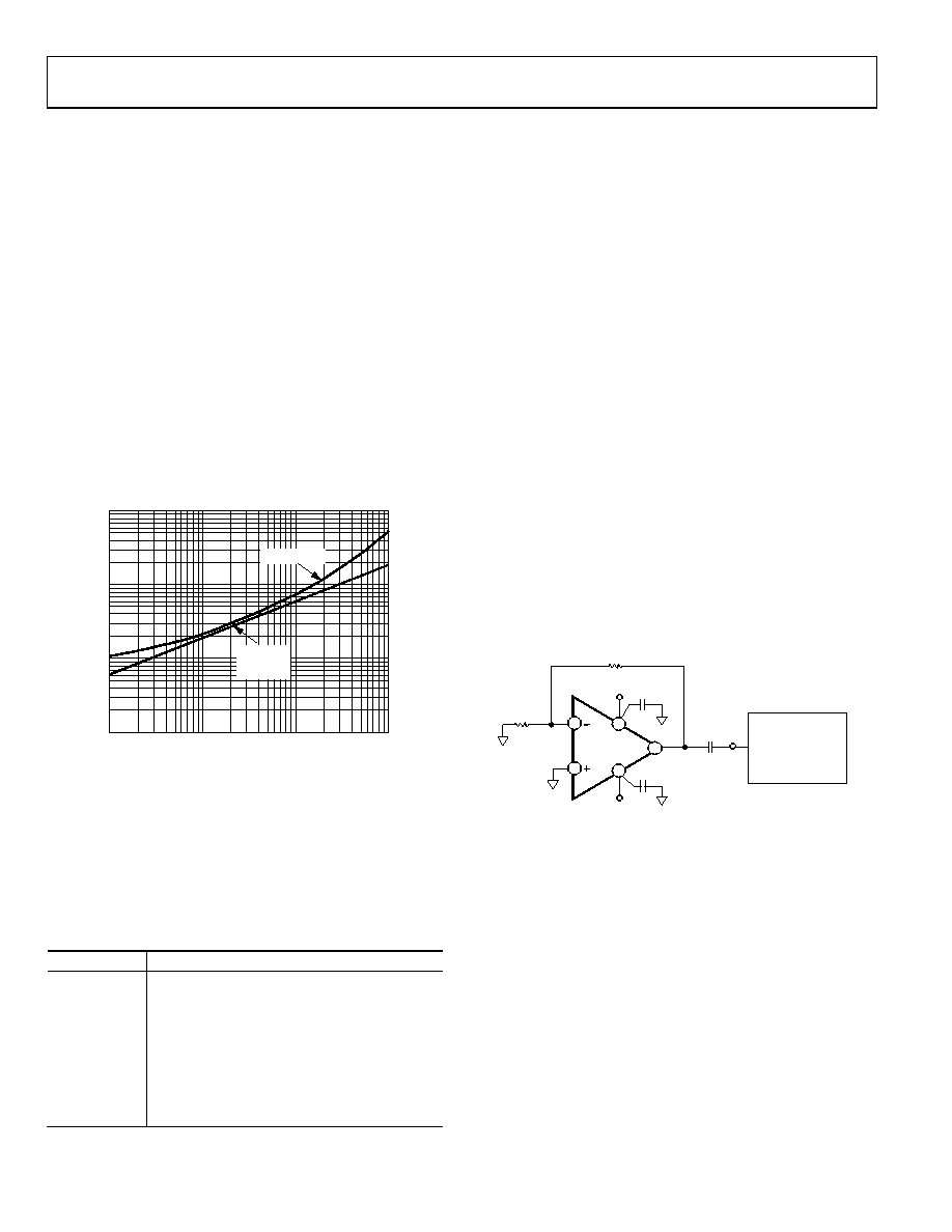
This equation is plotted for the AD797 in Figure 34. Because
optimum dc performance is obtained with matched source
resistances, this case is considered even though it is clear from
Equation 1 that eliminating the balancing source resistance
lowers the total noise by reducing the total RS by a factor of 2.
At very low source resistance (RS < 50 Ω), the voltage noise of the
amplifier dominates. As source resistance increases, the Johnson
noise of RS dominates until a higher resistance of RS > 2 kΩ is
achieved; the current noise component is larger than the
resistor noise.
00846-
033
100
1
0.1
10
100
1000
10000
SOURCE RESIST
ANCE ()
N
OIS
E(
nV
/√
H
z)
TOTAL NOISE
RESISTOR
NOISE
ONLY
Figure 34. Noise vs. Source Resistance
The AD797 is the optimum choice for low noise performance if
the source resistance is kept <1 kΩ. At higher values of source
resistance, optimum performance with respect to only noise is
obtained with other amplifiers from Analog Devices (Table 5).
For up to date information, see AN-940 at www.analog.com.
Table 5. Recommended Amplifiers for Different Source
Impedances
RS (k)
Recommended Amplifier
0 to <1
1 to <10
10 to <100
>100
LOW FREQUENCY NOISE
Analog Devices specifies low frequency noise as a peak-to-peak
quantity in a 0.1 Hz to 10 Hz bandwidth. Several techniques can
be used to make this measurement. The usual technique involves
amplifying, filtering, and measuring the amplifier noise for a
predetermined test time. The noise bandwidth of the filter is
corrected for, and the test time is carefully controlled because
the measurement time acts as an additional low frequency roll-off.
The plot in Figure 6 uses a slightly different technique: an FFT-
based instrument (Figure 35) is used to generate a 10 Hz brickwall
filter. A low frequency pole at 0.1 Hz is generated with an external
ac coupling capacitor, which is also the instrument being dc coupled.
Several precautions are necessary to attain optimum low
frequency noise performance:
Care must be used to account for the effects of RS. Even
a 10 Ω resistor has 0.4 nV/√Hz of noise (an error of 9%
when root sum squared with 0.9 nV/√Hz).
The test setup must be fully warmed up to prevent eOS drift
from erroneously contributing to input noise.
Circuitry must be shielded from air currents. Heat flow out
of the package through its leads creates the opportunity for
a thermoelectric potential at every junction of different metals.
Selective heating and cooling of these by random air currents
appears as 1/f noise and obscures the true device noise.
The results must be interpreted using valid statistical
techniques.
7
4
6
2
3
HP 3465
DYNAMIC SIGNAL
ANALYZER
(10Hz)
1
100k
*
VOUT
+VS
–VS
1.5F
AD797
00846-
034
*USE THE POWER SUPPLY BYPASSING SHOWN IN FIGURE 35.
Figure 35. Test Setup for Measuring 0.1 Hz to 10 Hz Noise
WIDEBAND NOISE
Due to its single-stage design, the noise of the AD797 is flat
over frequencies from less than 10 Hz to beyond 1 MHz. This
is not true of most dc precision amplifiers, where second-stage
noise contributes to input-referred noise beyond the audio
frequency range. The AD797 offers new levels of performance in
wideband imaging applications. In sampled data systems, where
aliasing of out-of-band noise into the signal band is a problem,
the AD797 outperforms all previously available IC op amps.
相关PDF资料 |
PDF描述 |
|---|---|
| FWJ-06-01-T-S | CONN HEADER .156" 6POS SNGL TIN |
| LT2079CS#TRPBF | IC OPAMP MICROPOWER QUAD 14SOIC |
| 57102-F08-21LF | MINITEK |
| LT2079CS#TR | IC OPAMP PREC QUAD MCRPWR 14SOIC |
| 0234004.MXBP | FUSE 5X20 C/CODE M 4A/250V |
相关代理商/技术参数 |
参数描述 |
|---|---|
| AD797ARZ | 功能描述:IC OPAMP GP 110MHZ ULDIST 8SOIC RoHS:是 类别:集成电路 (IC) >> Linear - Amplifiers - Instrumentation 系列:- 标准包装:1 系列:MicroAmplifier™ 放大器类型:通用 电路数:4 输出类型:- 转换速率:3.5 V/µs 增益带宽积:1MHz -3db带宽:- 电流 - 输入偏压:5pA 电压 - 输入偏移:1500µV 电流 - 电源:220µA 电流 - 输出 / 通道:60mA 电压 - 电源,单路/双路(±):4.5 V ~ 36 V,±2.25 V ~ 18 V 工作温度:-40°C ~ 85°C 安装类型:表面贴装 封装/外壳:14-SOIC(0.154",3.90mm 宽) 供应商设备封装:14-SOIC 包装:剪切带 (CT) 其它名称:296-29363-1 |
| AD797ARZ-REEL | 功能描述:IC OPAMP GP 110MHZ ULDIST 8SOIC RoHS:是 类别:集成电路 (IC) >> Linear - Amplifiers - Instrumentation 系列:- 标准包装:50 系列:- 放大器类型:J-FET 电路数:2 输出类型:- 转换速率:13 V/µs 增益带宽积:3MHz -3db带宽:- 电流 - 输入偏压:65pA 电压 - 输入偏移:3000µV 电流 - 电源:1.4mA 电流 - 输出 / 通道:- 电压 - 电源,单路/双路(±):7 V ~ 36 V,±3.5 V ~ 18 V 工作温度:-40°C ~ 85°C 安装类型:通孔 封装/外壳:8-DIP(0.300",7.62mm) 供应商设备封装:8-PDIP 包装:管件 |
| AD797ARZ-REEL7 | 功能描述:IC OPAMP GP 110MHZ ULDIST 8SOIC RoHS:是 类别:集成电路 (IC) >> Linear - Amplifiers - Instrumentation 系列:- 标准包装:150 系列:- 放大器类型:音频 电路数:2 输出类型:- 转换速率:5 V/µs 增益带宽积:12MHz -3db带宽:- 电流 - 输入偏压:100nA 电压 - 输入偏移:500µV 电流 - 电源:6mA 电流 - 输出 / 通道:50mA 电压 - 电源,单路/双路(±):4 V ~ 32 V,±2 V ~ 16 V 工作温度:-40°C ~ 85°C 安装类型:表面贴装 封装/外壳:8-TSSOP(0.173",4.40mm 宽) 供应商设备封装:8-TSSOP 包装:管件 |
| AD797BN | 制造商:Analog Devices 功能描述: |
| AD797BR | 功能描述:IC OPAMP GP 110MHZ ULDIST 8SOIC RoHS:否 类别:集成电路 (IC) >> Linear - Amplifiers - Instrumentation 系列:- 标准包装:2,500 系列:Excalibur™ 放大器类型:J-FET 电路数:1 输出类型:- 转换速率:45 V/µs 增益带宽积:10MHz -3db带宽:- 电流 - 输入偏压:20pA 电压 - 输入偏移:490µV 电流 - 电源:1.7mA 电流 - 输出 / 通道:48mA 电压 - 电源,单路/双路(±):4.5 V ~ 38 V,±2.25 V ~ 19 V 工作温度:-40°C ~ 85°C 安装类型:表面贴装 封装/外壳:8-SOIC(0.154",3.90mm 宽) 供应商设备封装:8-SOIC 包装:带卷 (TR) |
发布紧急采购,3分钟左右您将得到回复。