- 您现在的位置:买卖IC网 > PDF目录1985 > AD7985BCPZ-RL7 (Analog Devices Inc)IC ADC 16B 2.5MSPS PULSR 20LFCSP PDF资料下载
参数资料
| 型号: | AD7985BCPZ-RL7 |
| 厂商: | Analog Devices Inc |
| 文件页数: | 13/28页 |
| 文件大小: | 0K |
| 描述: | IC ADC 16B 2.5MSPS PULSR 20LFCSP |
| 标准包装: | 1,500 |
| 系列: | PulSAR® |
| 位数: | 16 |
| 采样率(每秒): | 2.5M |
| 数据接口: | DSP,MICROWIRE?,QSPI?,串行,SPI? |
| 转换器数目: | 1 |
| 功率耗散(最大): | 33mW |
| 电压电源: | 模拟和数字 |
| 工作温度: | -40°C ~ 85°C |
| 安装类型: | 表面贴装 |
| 封装/外壳: | 20-VFQFN 裸露焊盘,CSP |
| 供应商设备封装: | 20-LFCSP-VQ |
| 包装: | 带卷 (TR) |
| 输入数目和类型: | 1 个伪差分,单极 |
第1页第2页第3页第4页第5页第6页第7页第8页第9页第10页第11页第12页当前第13页第14页第15页第16页第17页第18页第19页第20页第21页第22页第23页第24页第25页第26页第27页第28页
AD7985
Rev. A | Page 20 of 28
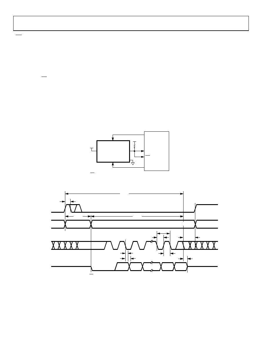
CS MODE, 3-WIRE WITH BUSY INDICATOR
This mode is usually used when a single AD7985 is connected
to an SPI-compatible digital host that has an interrupt input. It
is available only in normal conversion mode (TURBO is low).
The connection diagram is shown in Figure 28, and the corre-
sponding timing is given in Figure 29.
With SDI tied to VIO, a rising edge on CNV initiates a con-
version, selects CS mode, and forces SDO to high impedance.
SDO is maintained in high impedance until the completion of
the conversion, irrespective of the state of CNV. Prior to the
minimum conversion time, CNV can be used to select other SPI
devices, such as analog multiplexers, but CNV must be returned
low before the minimum conversion time elapses and then held
low for the maximum possible conversion time to guarantee the
generation of the busy signal indicator.
When the conversion is complete, SDO goes from high imped-
ance to low impedance. With a pull-up on the SDO line, this
transition can be used as an interrupt signal to initiate the data
readback controlled by the digital host. The AD7985 then enters
the acquisition phase and powers down. The data bits are then
clocked out, MSB first, by subsequent SCK falling edges. The
data is valid on both SCK edges. Although the rising edge can
be used to capture the data, a digital host using the SCK falling
edge allows a faster reading rate, provided that it has an acceptable
hold time. After the optional 17th SCK falling edge, SDO returns
to high impedance.
If multiple AD7985 devices are selected at the same time, the
SDO output pin handles this contention without damage or
induced latch-up. Meanwhile, it is recommended that this
contention be kept as short as possible to limit extra power
dissipation.
AD7985
SDI
SDO
CNV
SCK
CONVERT
DATA IN
CLK
DIGITAL HOST
VIO
IRQ
VIO
47k
TURBO
07947-
011
Figure 28. CS Mode, 3-Wire with Busy Indicator Connection Diagram (SDI High)
SDO
D15
D14
D1
D0
tDIS
SCK
1
2
3
15
16
17
tSCK
tSCKL
tSCKH
tHSDO
tDSDO
CNV
CONVERSION
ACQUISITION
tCONV
tCYC
ACQUISITION
TURBO = 0
SDI = 1
tCNVH
tACQ
tQUIET
(I/O QUIET
TIME)
07947-
012
Figure 29. CS Mode, 3-Wire with Busy Indicator Serial Interface Timing (SDI High)
相关PDF资料 |
PDF描述 |
|---|---|
| AD7986BCPZ-RL7 | IC ADC 18BIT 2MSPS SAR 20LFCSP |
| AD7988-1BRMZ-RL7 | IC ADC 16BIT SRL 100KSPS 10MSOP |
| AD7991YRJZ-1RL | IC ADC 12BIT 4CH I2C SOT23-8 |
| AD7992BRMZ-1REEL | IC ADC 12BIT 2CHAN I2C 10MSOP |
| AD7994BRUZ-1 | IC ADC 12BIT 4CHAN I2C 16TSSOP |
相关代理商/技术参数 |
参数描述 |
|---|---|
| AD7986 | 制造商:AD 制造商全称:Analog Devices 功能描述:1 nV/√Hz, Low Power |
| AD7986BCPZ | 功能描述:IC ADC 18BIT 2MSPS SAR 20LFCSP RoHS:是 类别:集成电路 (IC) >> 数据采集 - 模数转换器 系列:- 其它有关文件:TSA1204 View All Specifications 标准包装:1 系列:- 位数:12 采样率(每秒):20M 数据接口:并联 转换器数目:2 功率耗散(最大):155mW 电压电源:模拟和数字 工作温度:-40°C ~ 85°C 安装类型:表面贴装 封装/外壳:48-TQFP 供应商设备封装:48-TQFP(7x7) 包装:Digi-Reel® 输入数目和类型:4 个单端,单极;2 个差分,单极 产品目录页面:1156 (CN2011-ZH PDF) 其它名称:497-5435-6 |
| AD7986BCPZ-RL7 | 功能描述:IC ADC 18BIT 2MSPS SAR 20LFCSP RoHS:是 类别:集成电路 (IC) >> 数据采集 - 模数转换器 系列:- 标准包装:1 系列:- 位数:14 采样率(每秒):83k 数据接口:串行,并联 转换器数目:1 功率耗散(最大):95mW 电压电源:双 ± 工作温度:0°C ~ 70°C 安装类型:通孔 封装/外壳:28-DIP(0.600",15.24mm) 供应商设备封装:28-PDIP 包装:管件 输入数目和类型:1 个单端,双极 |
| AD7986BCPZ-U1 | 制造商:Analog Devices 功能描述:16-BIT, 10MSPS PULSAR DIFFERENTIAL ADC - Rail/Tube |
| AD7986XCPZ-U1 | 制造商:Analog Devices 功能描述:16-BIT, 10MSPS PULSAR DIFFERENTIAL ADC - Rail/Tube |
发布紧急采购,3分钟左右您将得到回复。