- 您现在的位置:买卖IC网 > PDF目录10327 > AD7994BRUZ-0REEL (Analog Devices Inc)IC ADC 12BIT 4CHAN I2C 16TSSOP PDF资料下载
参数资料
| 型号: | AD7994BRUZ-0REEL |
| 厂商: | Analog Devices Inc |
| 文件页数: | 22/32页 |
| 文件大小: | 0K |
| 描述: | IC ADC 12BIT 4CHAN I2C 16TSSOP |
| 标准包装: | 2,500 |
| 位数: | 12 |
| 采样率(每秒): | 188k |
| 数据接口: | I²C,串行 |
| 转换器数目: | 1 |
| 功率耗散(最大): | 2.2mW |
| 电压电源: | 单电源 |
| 工作温度: | -40°C ~ 125°C |
| 安装类型: | 表面贴装 |
| 封装/外壳: | 16-TSSOP(0.173",4.40mm 宽) |
| 供应商设备封装: | 16-TSSOP |
| 包装: | 带卷 (TR) |
| 输入数目和类型: | 4 个单端,单极 |
第1页第2页第3页第4页第5页第6页第7页第8页第9页第10页第11页第12页第13页第14页第15页第16页第17页第18页第19页第20页第21页当前第22页第23页第24页第25页第26页第27页第28页第29页第30页第31页第32页

AD7993/AD7994
Rev. 0 | Page 29 of 32
MODE 2—COMMAND MODE
This mode allows a conversion to be automatically initiated any
time a write operation occurs. In order to use this mode,
Command Bits C4 to C1 in the address pointer byte, shown in
Table 7, must be programmed.
To select a single analog input for conversion in this mode,
the user must set bits C4 to C1of the address pointer byte to
indicate which channel to convert (see Table 27). When all four
command bits are 0, this mode is not in use.
A sequence can also be set up for this mode. If more than one
command bit is set in the address pointer byte, the ADC starts
converting on the lowest channel in the sequence and then the
next lowest until all the channels in the sequence have been
converted. The ADC stops converting the sequence when it
receives a STOP bit.
Figure 29 illustrates a 2-byte read operation from the conver-
sion result register. This operation is normally preceded by a
write to the address pointer register so that the following read
accesses the desired register, in this case the conversion result
register (Figure 26). If Command Bits C4 to C1 are set when the
contents of the address pointer register are being loaded, the
AD7993/AD7994 begin to power up and convert the selected
channel(s). Power-up begins on the fifth SCL falling edge of the
address point byte (see Point A in Figure 33).
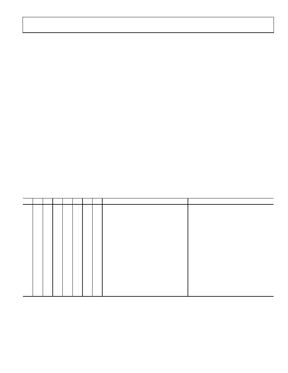
Table 27 shows the channel selection in this mode via
Command Bits C4 to C1 in the address pointer register. The
wake-up and conversion times combined should take
approximately 3 s. Following this, the AD7993/AD7994 must
be addressed again to indicate that a read operation is required.
The read then takes place from the conversion result register.
This read accesses the conversion result from the channel
selected via the command bits. If the Command Bits C2 and C1
were set to 1, 1, then a four byte read would be necessary. The
first read accesses the data from the conversion on VIN1. While
this read takes place, a conversion occurs on VIN2. The second
mode operates.
When operating the AD7994-1/AD7993-1 in Mode 2 with a
high speed mode, 3.4 MHz SCL, the conversion may not be
complete before the master tries to read the conversion result.
If this is the case, the AD7994-1/AD7993-1 hold the SCL line
low during the ACK clock after the read address until the con-
version is complete. When the conversion is complete, the
AD7994-1/AD7993-1 release the SCL line and the master can
then read the conversion result.
After the conversion is initiated by setting the command bits in
the address pointer byte, if the AD7993/AD7994 receive a stop
or NACK from the master, the devices stop converting.
Table 27. Address Pointer Byte
C4
C3
C2
C1
P3
P2
P1
P0
Mode 2, Convert On
Comments
0
Not selected
0
1
0
VIN1
0
1
0
VIN2
0
1
0
Sequence between VIN1 and VIN2
0
1
0
VIN3
0
1
0
1
0
Sequence between VIN1 and VIN3
0
1
0
Sequence between VIN2 and VIN3
0
1
0
Sequence between VIN1, VIN2, and VIN3
1
0
VIN4
1
0
1
0
Sequence between VIN1 and VIN4
1
0
1
0
Sequence between VIN2 and VIN4
1
0
1
0
Sequence between VIN1, VIN2, and VIN4
1
0
Sequence between VIN3 and VIN4
1
0
1
0
Sequence between VIN1, VIN3, and VIN4
1
0
Sequence between VIN2, VIN3, and VIN4
1
0
Sequence between VIN1, VIN2, VIN3, and VIN4
With the pointer bits set to all 0s, the next
read accesses the results of the conversion
result register.
相关PDF资料 |
PDF描述 |
|---|---|
| VI-B3W-IX-B1 | CONVERTER MOD DC/DC 5.5V 75W |
| VI-24H-IU-S | CONVERTER MOD DC/DC 52V 200W |
| VI-2WH-MX-S | CONVERTER MOD DC/DC 52V 75W |
| VI-24F-IU-S | CONVERTER MOD DC/DC 72V 200W |
| VI-24D-IU-S | CONVERTER MOD DC/DC 85V 200W |
相关代理商/技术参数 |
参数描述 |
|---|---|
| AD7994BRUZ-1 | 功能描述:IC ADC 12BIT 4CHAN I2C 16TSSOP RoHS:是 类别:集成电路 (IC) >> 数据采集 - 模数转换器 系列:- 标准包装:1,000 系列:- 位数:16 采样率(每秒):45k 数据接口:串行 转换器数目:2 功率耗散(最大):315mW 电压电源:模拟和数字 工作温度:0°C ~ 70°C 安装类型:表面贴装 封装/外壳:28-SOIC(0.295",7.50mm 宽) 供应商设备封装:28-SOIC W 包装:带卷 (TR) 输入数目和类型:2 个单端,单极 |
| AD7994BRUZ-1REEL | 功能描述:IC ADC 12BIT 4CHAN I2C 16TSSOP RoHS:是 类别:集成电路 (IC) >> 数据采集 - 模数转换器 系列:- 标准包装:1,000 系列:- 位数:16 采样率(每秒):45k 数据接口:串行 转换器数目:2 功率耗散(最大):315mW 电压电源:模拟和数字 工作温度:0°C ~ 70°C 安装类型:表面贴装 封装/外壳:28-SOIC(0.295",7.50mm 宽) 供应商设备封装:28-SOIC W 包装:带卷 (TR) 输入数目和类型:2 个单端,单极 |
| AD7994-X | 制造商:AD 制造商全称:Analog Devices 功能描述:4-Channel, 10- and 12-Bit ADCs with I2C Compatible Interface in 16-Lead TSSOP |
| AD7995 | 制造商:AD 制造商全称:Analog Devices 功能描述:4-Channel, 12-/10-/8-Bit ADC with I2C-Compatible Interface in 8-Lead SOT-23 |
| AD7995ARJZ-0RL | 功能描述:IC ADC 10BIT 4CHAN I2C SOT23-8 RoHS:是 类别:集成电路 (IC) >> 数据采集 - 模数转换器 系列:- 其它有关文件:TSA1204 View All Specifications 标准包装:1 系列:- 位数:12 采样率(每秒):20M 数据接口:并联 转换器数目:2 功率耗散(最大):155mW 电压电源:模拟和数字 工作温度:-40°C ~ 85°C 安装类型:表面贴装 封装/外壳:48-TQFP 供应商设备封装:48-TQFP(7x7) 包装:Digi-Reel® 输入数目和类型:4 个单端,单极;2 个差分,单极 产品目录页面:1156 (CN2011-ZH PDF) 其它名称:497-5435-6 |
发布紧急采购,3分钟左右您将得到回复。