参数资料
| 型号: | AD8000YCPZ-REEL7 |
| 厂商: | Analog Devices Inc |
| 文件页数: | 18/21页 |
| 文件大小: | 0K |
| 描述: | IC OPAMP CF LN 100MA 8SFCSP |
| 产品培训模块: | Practical Guide High Speed PCB Layout |
| 标准包装: | 1 |
| 放大器类型: | 电流反馈 |
| 电路数: | 1 |
| 转换速率: | 4100 V/µs |
| -3db带宽: | 1.35GHz |
| 电流 - 输入偏压: | 5µA |
| 电压 - 输入偏移: | 1000µV |
| 电流 - 电源: | 13.5mA |
| 电流 - 输出 / 通道: | 100mA |
| 电压 - 电源,单路/双路(±): | 4.5 V ~ 12 V,±2.25 V ~ 6 V |
| 工作温度: | -40°C ~ 125°C |
| 安装类型: | 表面贴装 |
| 封装/外壳: | 8-VFDFN 裸露焊盘,CSP |
| 供应商设备封装: | 8-LFCSP-VD(3x3) |
| 包装: | 标准包装 |
| 产品目录页面: | 769 (CN2011-ZH PDF) |
| 其它名称: | AD8000YCPZ-REEL7DKR |
Data Sheet
AD8000
Rev. B | Page 5 of 20
ABSOLUTE MAXIMUM RATINGS
Table 3.
Parameter
Rating
Supply Voltage
12.6 V
Power Dissipation
Common-Mode Input Voltage
VS 0.7 V to +VS + 0.7 V
Differential Input Voltage
±VS
Storage Temperature
65°C to +125°C
Operating Temperature Range
40°C to +125°C
Lead Temperature Range
(Soldering, 10 sec)
300°C
Junction Temperature
150°C
Stresses above those listed under Absolute Maximum Ratings
may cause permanent damage to the device. This is a stress
rating only; functional operation of the device at these or any
other conditions above those indicated in the operational
section of this specification is not implied. Exposure to absolute
maximum rating conditions for extended periods may affect
device reliability.
THERMAL RESISTANCE
θJA is specified for the worst-case conditions, that is, θJA is speci-
fied for device soldered in the circuit board for surface-mount
packages.
Table 4. Thermal Resistance
Package Type
θJA
θJC
Unit
SOIC-8
80
30
°C/W
3 mm × 3 mm LFCSP
93
35
°C/W
Maximum Power Dissipation
The maximum safe power dissipation for the AD8000 is limited
by the associated rise in junction temperature (TJ) on the die. At
approximately 150°C, which is the glass transition temperature,
the properties of the plastic change. Even temporarily exceeding
this temperature limit can change the stresses that the package
exerts on the die, permanently shifting the parametric perfor-
mance of the AD8000. Exceeding a junction temperature of
175°C for an extended period of time can result in changes
in silicon devices, potentially causing degradation or loss of
functionality.
The power dissipated in the package (PD) is the sum of the
quiescent power dissipation and the power dissipated in the die
due to the AD8000 drive at the output. The quiescent power is
the voltage between the supply pins (VS) times the quiescent
current (IS).
PD = Quiescent Power + (Total Drive Power – Load Power)
(
)
L
2
OUT
L
OUT
S
D
R
V
–
R
V
2
V
I
V
P
×
+
×
=
RMS output voltages should be considered. If RL is referenced
to VS, as in single-supply operation, the total drive power is
VS × IOUT. If the rms signal levels are indeterminate, consider
the worst case, when VOUT = VS/4 for RL to midsupply.
(
) (
)
L
S
D
R
/
V
I
V
P
2
4
+
×
=
In single-supply operation with RL referenced to VS, worst case
is VOUT = VS/2.
Airflow increases heat dissipation, effectively reducing θJA.
Also, more metal directly in contact with the package leads and
exposed paddle from metal traces, through holes, ground, and
power planes reduces θJA.
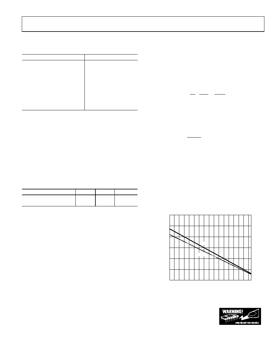
Figure 4 shows the maximum safe power dissipation in the
package vs. the ambient temperature for the exposed paddle
SOIC (80°C/W) and the LFCSP (93°C/W) package on a JEDEC
standard 4-layer board. θJA values are approximations.
0
0.5
1.0
1.5
2.0
2.5
3.0
MAXIMUM
POWER
DISSIPATION
(W)
05321-063
–30 –20 –10
0
10
20
40
80
30
50
60
70
100
90
120
110
AMBIENT TEMPERATURE (
°C)
SOIC
LFCSP
–40
Figure 4. Maximum Power Dissipation vs. Temperature for a 4-Layer Board
ESD CAUTION
ESD (electrostatic discharge) sensitive device. Electrostatic charges as high as 4000 V readily accumulate
on the human body and test equipment and can discharge without detection. Although this product features
proprietary ESD protection circuitry, permanent damage may occur on devices subjected to high energy elec-
trostatic discharges. Therefore, proper ESD precautions are recommended to avoid performance degradation
and loss of functionality.
相关PDF资料 |
PDF描述 |
|---|---|
| AD8668ARUZ-REEL | IC OPAMP GP R-R 4MHZ LN 14TSSOP |
| TSW-117-14-T-S | CONN HEADER 17POS .100" SNGL TIN |
| AD8672ARMZ-REEL | IC OPAMP GP 10MHZ DUAL LN 8MSOP |
| SFM-120-02-S-D | CONN RECEPT 40POS .050" SMT |
| ESW-124-33-G-D | CONN SOCKET .100" 48POS PCB DUAL |
相关代理商/技术参数 |
参数描述 |
|---|---|
| AD8000YRD-EBZ | 功能描述:BOARD EVAL FOR AD8000YRD RoHS:是 类别:编程器,开发系统 >> 评估板 - 运算放大器 系列:- 产品培训模块:Lead (SnPb) Finish for COTS Obsolescence Mitigation Program 标准包装:1 系列:- |
| AD8000YRD-EBZ | 制造商:Analog Devices 功能描述:AD8000YRD-EBZ"A00973"EB-O8REDF-1Z |
| AD8000YRDZ | 功能描述:IC OPAMP CF LN 100MA 8SOIC RoHS:是 类别:集成电路 (IC) >> Linear - Amplifiers - Instrumentation 系列:- 产品培训模块:Differential Circuit Design Techniques for Communication Applications 标准包装:1 系列:- 放大器类型:RF/IF 差分 电路数:1 输出类型:差分 转换速率:9800 V/µs 增益带宽积:- -3db带宽:2.9GHz 电流 - 输入偏压:3µA 电压 - 输入偏移:- 电流 - 电源:40mA 电流 - 输出 / 通道:- 电压 - 电源,单路/双路(±):3 V ~ 3.6 V 工作温度:-40°C ~ 85°C 安装类型:表面贴装 封装/外壳:16-VQFN 裸露焊盘,CSP 供应商设备封装:16-LFCSP-VQ 包装:剪切带 (CT) 产品目录页面:551 (CN2011-ZH PDF) 其它名称:ADL5561ACPZ-R7CT |
| AD8000YRDZ-REEL | 功能描述:IC OPAMP CF LN 100MA 8SOIC RoHS:是 类别:集成电路 (IC) >> Linear - Amplifiers - Instrumentation 系列:- 标准包装:50 系列:- 放大器类型:通用 电路数:2 输出类型:满摆幅 转换速率:1.8 V/µs 增益带宽积:6.5MHz -3db带宽:4.5MHz 电流 - 输入偏压:5nA 电压 - 输入偏移:100µV 电流 - 电源:65µA 电流 - 输出 / 通道:35mA 电压 - 电源,单路/双路(±):1.8 V ~ 5.25 V,±0.9 V ~ 2.625 V 工作温度:-40°C ~ 85°C 安装类型:表面贴装 封装/外壳:10-TFSOP,10-MSOP(0.118",3.00mm 宽) 供应商设备封装:10-MSOP 包装:管件 |
| AD8000YRDZ-REEL7 | 功能描述:IC OPAMP CF LN 100MA 8SOIC RoHS:是 类别:集成电路 (IC) >> Linear - Amplifiers - Instrumentation 系列:- 标准包装:50 系列:- 放大器类型:通用 电路数:2 输出类型:满摆幅 转换速率:1.8 V/µs 增益带宽积:6.5MHz -3db带宽:4.5MHz 电流 - 输入偏压:5nA 电压 - 输入偏移:100µV 电流 - 电源:65µA 电流 - 输出 / 通道:35mA 电压 - 电源,单路/双路(±):1.8 V ~ 5.25 V,±0.9 V ~ 2.625 V 工作温度:-40°C ~ 85°C 安装类型:表面贴装 封装/外壳:10-TFSOP,10-MSOP(0.118",3.00mm 宽) 供应商设备封装:10-MSOP 包装:管件 |
发布紧急采购,3分钟左右您将得到回复。