参数资料
| 型号: | AD8000YRDZ |
| 厂商: | Analog Devices Inc |
| 文件页数: | 8/21页 |
| 文件大小: | 0K |
| 描述: | IC OPAMP CF LN 100MA 8SOIC |
| 产品培训模块: | Practical Guide High Speed PCB Layout |
| 标准包装: | 98 |
| 放大器类型: | 电流反馈 |
| 电路数: | 1 |
| 转换速率: | 4100 V/µs |
| -3db带宽: | 1.58GHz |
| 电流 - 输入偏压: | 5µA |
| 电压 - 输入偏移: | 1000µV |
| 电流 - 电源: | 13.5mA |
| 电流 - 输出 / 通道: | 100mA |
| 电压 - 电源,单路/双路(±): | 4.5 V ~ 12 V,±2.25 V ~ 6 V |
| 工作温度: | -40°C ~ 125°C |
| 安装类型: | 表面贴装 |
| 封装/外壳: | 8-SOIC(0.154",3.90mm Width)裸露焊盘 |
| 供应商设备封装: | 8-SOIC-EP |
| 包装: | 管件 |
| 产品目录页面: | 769 (CN2011-ZH PDF) |
Data Sheet
AD8000
Rev. B | Page 15 of 20
LOW DISTORTION PINOUT
The AD8000 LFCSP features ADI’s new low distortion pinout.
The new pinout lowers the second harmonic distortion and
simplifies the circuit layout. The close proximity of the non-
inverting input and the negative supply pin creates a source of
second harmonic distortion. Physical separation of the non-
inverting input pin and the negative power supply pin reduces
this distortion significantly, as seen in Figure 22.
By providing an additional output pin, the feedback resistor
can be connected directly across Pin 2 and Pin 3. This greatly
simplifies the routing of the feedback resistor and allows a more
compact circuit layout, which reduces its size and helps to min-
imize parasitics and increase stability.
The SOIC also features a dedicated feedback pin. The feedback
pin is brought out on Pin 1, which is typically a No Connect on
standard SOIC pinouts.
Existing applications that use the standard SOIC pinout can
take full advantage of the performance offered by the AD8000.
For drop-in replacements, ensure that Pin 1 is not connected to
ground or to any other potential because this pin is connected
internally to the output of the amplifier. For existing designs,
Pin 6 can still be used for the feedback resistor.
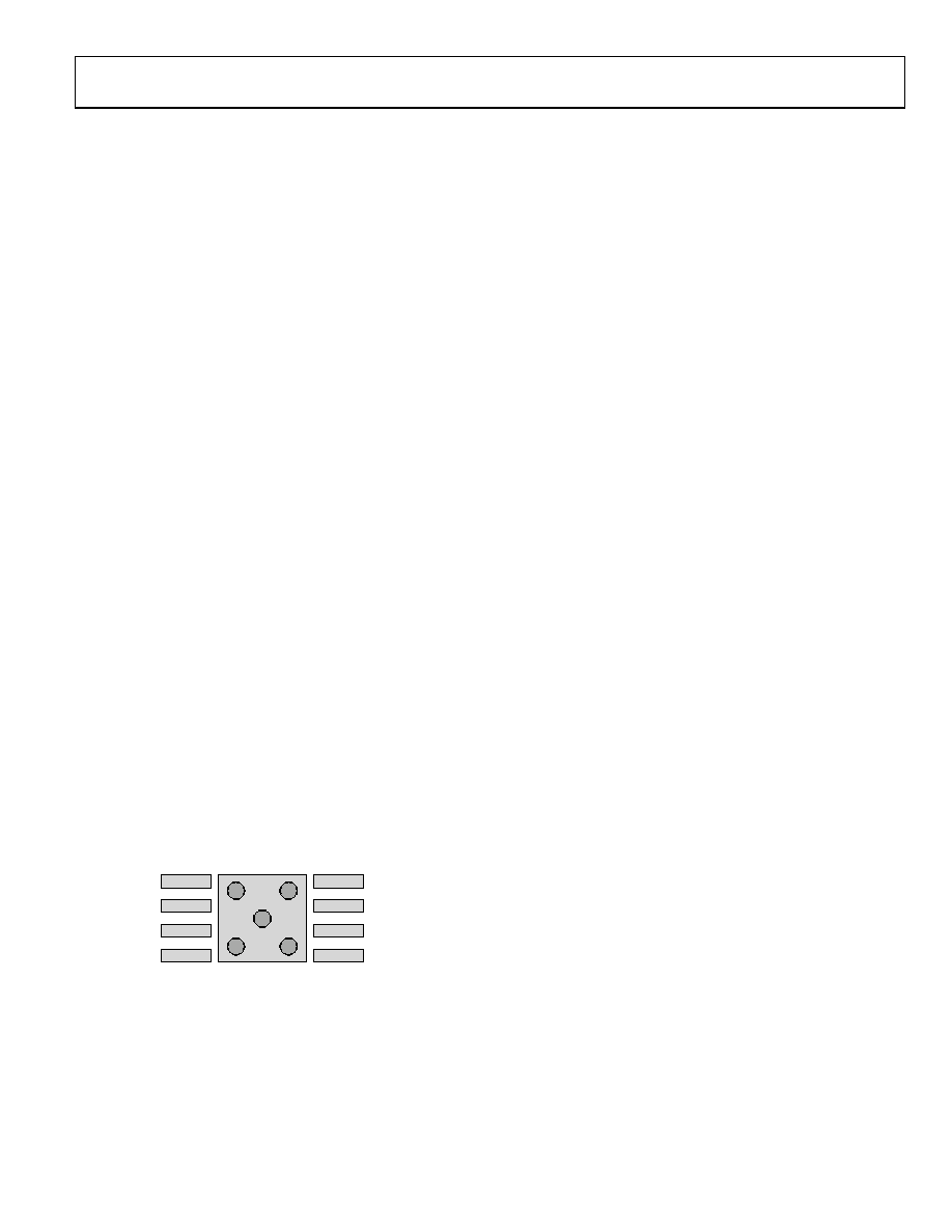
EXPOSED PADDLE
The AD8000 features an exposed paddle, which can lower the
thermal resistance by 25% compared to a standard SOIC plastic
package. The paddle can be soldered directly to the ground plane
of the board. Figure 53 shows a typical pad geometry for the
LFCSP, the same type of pad geometry can be applied to the
SOIC package.
Thermal vias or “heat pipes” can also be incorporated into the
design of the mounting pad for the exposed paddle. These addi-
tional vias improve the thermal transfer from the package to
the PCB. Using a heavier weight copper on the surface to which
the amplifier’s exposed paddle is soldered also reduces the over-
all thermal resistance “seen” by the AD8000.
05321-034
Figure 53. LFCSP Exposed Paddle Layout
PRINTED CIRCUIT BOARD LAYOUT
Laying out the printed circuit board (PCB) is usually the last
step in the design process and often proves to be one of the
most critical. A brilliant design can be rendered useless because
of a poor or sloppy layout. Since the AD8000 can operate into
the RF frequency spectrum, high frequency board layout con-
siderations must be taken into account. The PCB layout, signal
routing, power supply bypassing, and grounding all must be
addressed to ensure optimal performance.
SIGNAL ROUTING
The AD8000 LFCSP features the new low distortion pinout
with a dedicated feedback pin and allows a compact layout. The
dedicated feedback pin reduces the distance from the output to
the inverting input, which greatly simplifies the routing of the
feedback network.
To minimize parasitic inductances, ground planes should be
used under high frequency signal traces. However, the ground
plane should be removed from under the input and output pins
to minimize the formation of parasitic capacitors, which
degrades phase margin. Signals that are susceptible to noise
pickup should be run on the internal layers of the PCB, which
can provide maximum shielding.
POWER SUPPLY BYPASSING
Power supply bypassing is a critical aspect of the PCB design
process. For best performance, the AD8000 power supply pins
need to be properly bypassed.
A parallel connection of capacitors from each of the power
supply pins to ground works best. Paralleling different values
and sizes of capacitors helps to ensure that the power supply
pins “see” a low ac impedance across a wide band of frequen-
cies. This is important for minimizing the coupling of noise into
the amplifier. Starting directly at the power supply pins, the
smallest value and sized component should be placed on the
same side of the board as the amplifier, and as close as possible
to the
amplifier, and connected to the ground plane. This process
should be repeated for the next larger value capacitor. It is
recommended for the AD8000 that a 0.1 F ceramic 0508 case
be used. The 0508 offers low series inductance and excellent
high frequency performance. The 0.1 F case provides low
impedance at high frequencies. A 10 F electrolytic capacitor
should be placed in parallel with the 0.1 F. The 10 f capacitor
provides low ac impedance at low frequencies. Smaller values
of electrolytic capacitors can be used, depending on the circuit
requirements. Additional smaller value capacitors help to
provide a low impedance path for unwanted noise out to higher
frequencies but are not always necessary.
相关PDF资料 |
PDF描述 |
|---|---|
| SMCJ16A | TVS UNIDIRECT 1500W 16V SMC |
| LTC2051CS8#PBF | IC OPAMP ZERO DRIFT DUAL 8SOIC |
| SMCJ28A | TVS UNIDIRECT 1500W 28V SMC |
| 929834-01-27-RK | CONN HEADER 27POS SNGL .100 STR |
| 9-146253-0-03 | CONN HDR BRKWAY .100 06POS VERT |
相关代理商/技术参数 |
参数描述 |
|---|---|
| AD8000YRDZ-REEL | 功能描述:IC OPAMP CF LN 100MA 8SOIC RoHS:是 类别:集成电路 (IC) >> Linear - Amplifiers - Instrumentation 系列:- 标准包装:50 系列:- 放大器类型:通用 电路数:2 输出类型:满摆幅 转换速率:1.8 V/µs 增益带宽积:6.5MHz -3db带宽:4.5MHz 电流 - 输入偏压:5nA 电压 - 输入偏移:100µV 电流 - 电源:65µA 电流 - 输出 / 通道:35mA 电压 - 电源,单路/双路(±):1.8 V ~ 5.25 V,±0.9 V ~ 2.625 V 工作温度:-40°C ~ 85°C 安装类型:表面贴装 封装/外壳:10-TFSOP,10-MSOP(0.118",3.00mm 宽) 供应商设备封装:10-MSOP 包装:管件 |
| AD8000YRDZ-REEL7 | 功能描述:IC OPAMP CF LN 100MA 8SOIC RoHS:是 类别:集成电路 (IC) >> Linear - Amplifiers - Instrumentation 系列:- 标准包装:50 系列:- 放大器类型:通用 电路数:2 输出类型:满摆幅 转换速率:1.8 V/µs 增益带宽积:6.5MHz -3db带宽:4.5MHz 电流 - 输入偏压:5nA 电压 - 输入偏移:100µV 电流 - 电源:65µA 电流 - 输出 / 通道:35mA 电压 - 电源,单路/双路(±):1.8 V ~ 5.25 V,±0.9 V ~ 2.625 V 工作温度:-40°C ~ 85°C 安装类型:表面贴装 封装/外壳:10-TFSOP,10-MSOP(0.118",3.00mm 宽) 供应商设备封装:10-MSOP 包装:管件 |
| AD8001 | 制造商:AD 制造商全称:Analog Devices 功能描述:800 MHz, 50 mW Current Feedback Amplifier |
| AD8001_03 | 制造商:AD 制造商全称:Analog Devices 功能描述:800 MHz, 50 mW Current Feedback Amplifier |
| AD800-10-TO5I | 功能描述:光电二极管 800um active area APD chip w/ IR RoHS:否 制造商:Vishay Semiconductors 产品:Photodiodes 反向电压:10 V 最大暗电流:30 nA 峰值波长:565 nm 上升时间:3.1 us 下降时间:3 us 半强度角度:50 deg 封装 / 箱体:TO-5 |
发布紧急采购,3分钟左右您将得到回复。