参数资料
| 型号: | AD8002ANZ |
| 厂商: | Analog Devices Inc |
| 文件页数: | 7/21页 |
| 文件大小: | 0K |
| 描述: | IC OPAMP CF DUAL LP LDIST 8DIP |
| 标准包装: | 50 |
| 放大器类型: | 电流反馈 |
| 电路数: | 2 |
| 转换速率: | 1200 V/µs |
| -3db带宽: | 600MHz |
| 电流 - 输入偏压: | 5µA |
| 电压 - 输入偏移: | 2000µV |
| 电流 - 电源: | 10mA |
| 电流 - 输出 / 通道: | 70mA |
| 电压 - 电源,单路/双路(±): | ±3 V ~ 6 V |
| 工作温度: | -40°C ~ 85°C |
| 安装类型: | 通孔 |
| 封装/外壳: | 8-DIP(0.300",7.62mm) |
| 供应商设备封装: | 8-PDIP |
| 包装: | 管件 |
REV. D
AD8002
–14–
Table I. Recommended Component Values
AD8002AN (DIP)
AD8002AR (SOIC)
Gain
Component
–10
–2
–1
+1
+2
+10
+100
–10
–2
–1
+1
+2
+10
+100
RF (
)
499
549
576
1210
750
499
1000
499
549
953
681
499
1000
RG (
)
49.9
274
576
–
750
54.9
10
49.9
249
549
–
681
54.9
10
RBT (Nominal) (
)
49.9
RC (
)*
75
0
75
0
RS (
)
49.9
RT (Nominal) (
)
–
61.9
54.9
49.9
–
61.9
54.9
49.9
Small Signal BW (MHz)
270
380
410
600
500
170
17
250
410
600
500
170
17
0.1 dB Flatness (MHz)
45
80
130
35
60
24
3
50
100
35
90
24
3
AD8002ARM ( SOIC)
Gain
Component
–10
–2
–1
+1
+2
+10
+100
RF (
)
499
590
1000
681
499
1000
RG (
)
49.9
249
590
–
681
54.9
10
RBT (Nominal) (
)
49.9
RC (
)*
75
0
RS (
)
49.9
RT (Nominal) (
)
–
61.9
49.9
Small Signal BW (MHz)
270
400
410
600
450
170
19
0.1 dB Flatness (MHz)
60
100
35
70
35
3
*RC is recommended to reduce peaking, and minimizes input reflections at frequencies above 300 MHz. However, R C is not required.
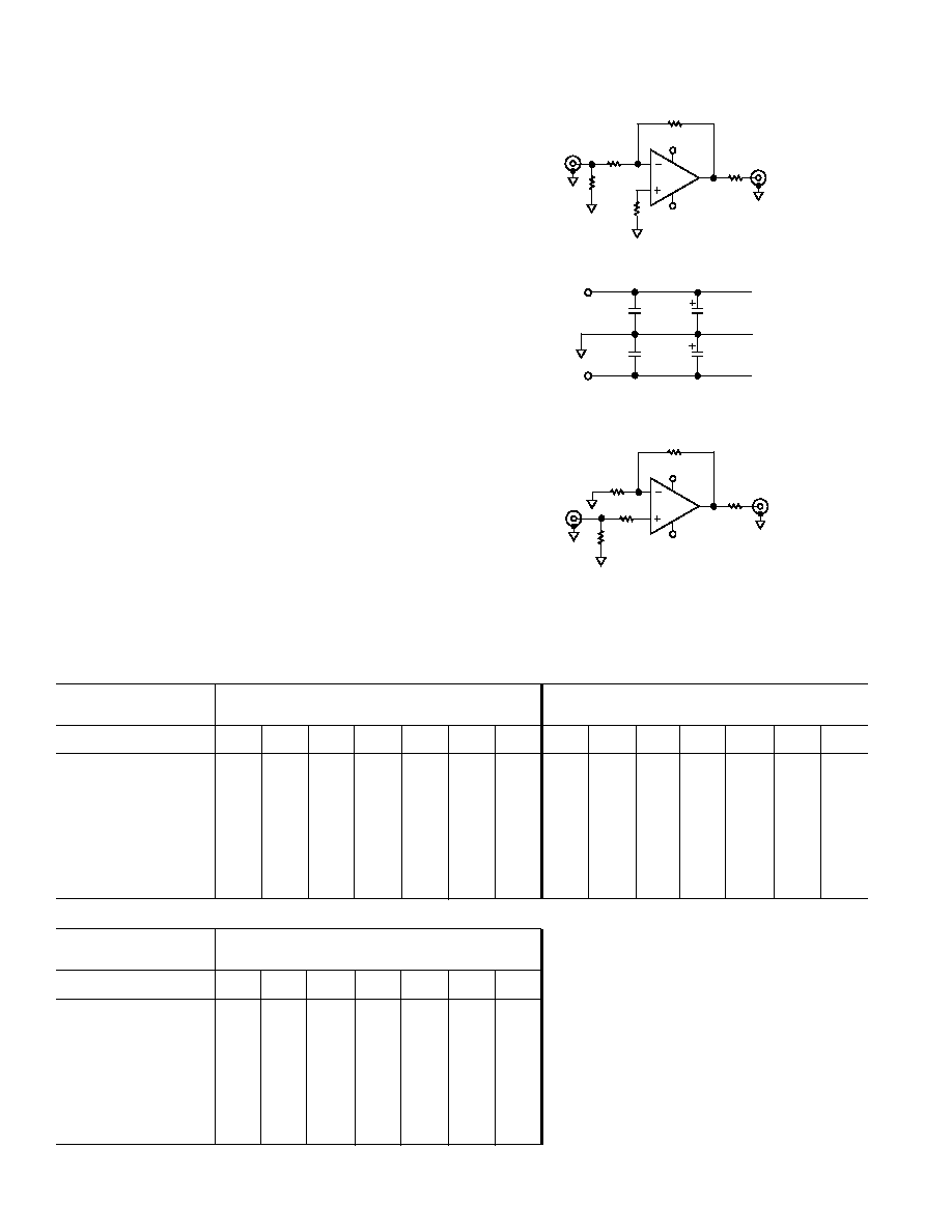
Layout Considerations
The specified high-speed performance of the AD8002 requires
careful attention to board layout and component selection.
Proper RF design techniques and low parasitic component selec-
tion are mandatory.
The PCB should have a ground plane covering all unused por-
tions of the component side of the board to provide a low
impedance ground path. The ground plane should be removed
from the area near the input pins to reduce stray capacitance.
Chip capacitors should be used for supply bypassing (see Figure
13). One end should be connected to the ground plane and the
other within 1/8 in. of each power pin. An additional large tanta-
lum electrolytic capacitor (4.7
F–10 F) should be connected in
parallel, but not necessarily so close, to supply current for fast,
large-signal changes at the output.
The feedback resistor should be located close to the inverting
input pin in order to keep the stray capacitance at this node to a
minimum. Capacitance variations of less than 1 pF at the invert-
ing input will significantly affect high-speed performance.
Stripline design techniques should be used for long signal traces
(greater than about 1 in.). These should be designed with a
characteristic impedance of 50
or 75 and be properly termi-
nated at each end.
Inverting Configuration
Supply Bypassing
Noninverting Configuration
RF
RBT
IN
+VS
–VS
RS
RT
RG
OUT
C1
0.1 F
C3
10 F
C2
0.1 F
C4
10 F
+VS
–VS
RF
RBT
IN
+VS
–VS
RT
RG
OUT
*RC
*SEE TABLE I
Figure 13. Inverting and Noninverting Configurations
相关PDF资料 |
PDF描述 |
|---|---|
| SMBJ24CA/54 | TVS J-LEAD 600W 24V BI-DIR SMD |
| SY88309BLMG | IC AMP PECL LIMITING POST 16-MLF |
| SMBJ20CA/54 | TVS J-LEAD 600W 20V BI-DIR SMD |
| SY88305BLMG | IC AMP CML LIMITING POST 16-MLF |
| SMBJ17CA/54 | TVS J-LEAD 600W 17V BI-DIR SMD |
相关代理商/技术参数 |
参数描述 |
|---|---|
| AD8002AR | 功能描述:IC OPAMP CF DUAL LP LDIST 8SOIC RoHS:否 类别:集成电路 (IC) >> Linear - Amplifiers - Instrumentation 系列:- 标准包装:150 系列:- 放大器类型:音频 电路数:2 输出类型:- 转换速率:5 V/µs 增益带宽积:12MHz -3db带宽:- 电流 - 输入偏压:100nA 电压 - 输入偏移:500µV 电流 - 电源:6mA 电流 - 输出 / 通道:50mA 电压 - 电源,单路/双路(±):4 V ~ 32 V,±2 V ~ 16 V 工作温度:-40°C ~ 85°C 安装类型:表面贴装 封装/外壳:8-TSSOP(0.173",4.40mm 宽) 供应商设备封装:8-TSSOP 包装:管件 |
| AD8002AR-EBZ | 功能描述:BOARD EVAL FOR AD8002AR RoHS:是 类别:编程器,开发系统 >> 评估板 - 运算放大器 系列:- 产品培训模块:Lead (SnPb) Finish for COTS Obsolescence Mitigation Program 标准包装:1 系列:- |
| AD8002ARM | 制造商:Analog Devices 功能描述:OP Amp Dual Current Fdbk 制造商:Analog Devices 功能描述:OP Amp Dual Current Fdbk ±6V/12V 8-Pin MSOP Tube 制造商:Rochester Electronics LLC 功能描述:MINISO DUAL HI PERF LO PWR VIDEO - Bulk |
| AD8002ARM-EBZ | 功能描述:BOARD EVAL FOR AD8002ARM RoHS:是 类别:编程器,开发系统 >> 评估板 - 运算放大器 系列:- 产品培训模块:Lead (SnPb) Finish for COTS Obsolescence Mitigation Program 标准包装:1 系列:- |
| AD8002ARM-REEL | 制造商:Analog Devices 功能描述:OP Amp Dual Current Fdbk 制造商:Rochester Electronics LLC 功能描述:MINISO DUAL HI PERF LO PWR VIDEO - Tape and Reel |
发布紧急采购,3分钟左右您将得到回复。