参数资料
| 型号: | AD8010ARZ-16 |
| 厂商: | Analog Devices Inc |
| 文件页数: | 11/12页 |
| 文件大小: | 0K |
| 描述: | IC OPAMP CF 200MA LP 16SOIC |
| 标准包装: | 47 |
| 放大器类型: | 电流反馈 |
| 电路数: | 1 |
| 转换速率: | 800 V/µs |
| -3db带宽: | 230MHz |
| 电流 - 输入偏压: | 10µA |
| 电压 - 输入偏移: | 5000µV |
| 电流 - 电源: | 15.5mA |
| 电流 - 输出 / 通道: | 200mA |
| 电压 - 电源,单路/双路(±): | 9 V ~ 12 V,±4.5 V ~ 6 V |
| 工作温度: | -40°C ~ 85°C |
| 安装类型: | 表面贴装 |
| 封装/外壳: | 16-SOIC(0.295",7.50mm 宽) |
| 供应商设备封装: | 16-SOIC W |
| 包装: | 管件 |
AD8010
–8–
REV. B
0
VOLTS
INPUT (500mV/DIV)
OUTPUT (1V/DIV)
G = +6
RF = 604
RL = 18.75
INPUT
OUTPUT
100ns
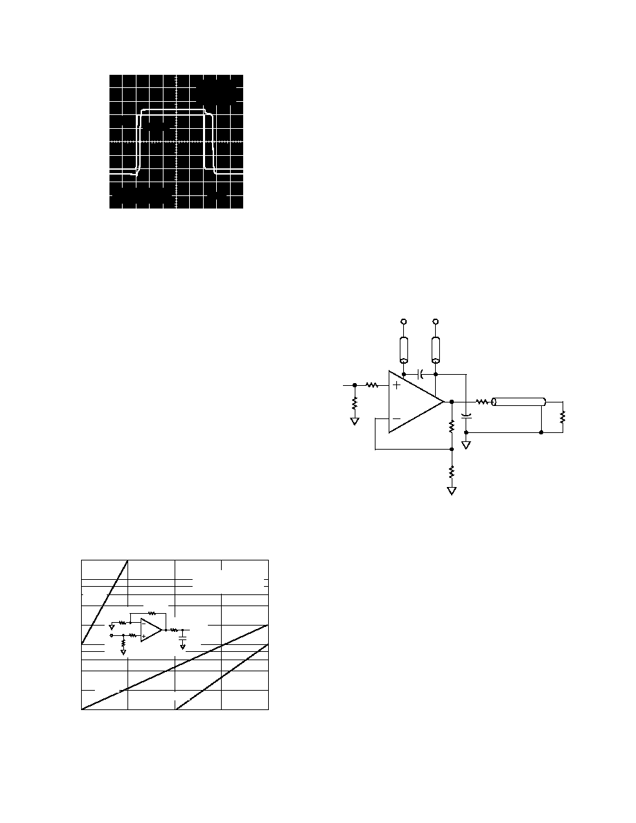
Figure 27. Overdrive Recovery; G = +6
OVERDRIVE RECOVERY
Overdrive of an amplifier occurs when the output and/or input
range are exceeded. The amplifier must recover from this over-
drive condition. As shown in Figure 27, the AD8010 recovers
within 35 ns from negative overdrive and within 75 ns from
positive overdrive.
THEORY OF OPERATION
The AD8010 is a current feedback amplifier optimized for high
current output while maintaining excellent performance with
respect to flatness, distortion and differential gain/phase. As a
video distribution amplifier, the AD8010 will drive up to 12
parallel video loads (12.5
) from a single output with 0.04%
differential gain and 0.04
° differential phase errors. This means
that, unlike designs with one driver per output, any output is a
true reflection of the signal on all other outputs.
The high output current capability of the AD8010 also make it
useful in xDSL applications. The AD8010 can drive a 12.5
single-ended or 25
differential load with low harmonic dis-
tortion. This makes it useful in designs that utilize a step-up
transformer to drive a twisted-pair transmission line.
To achieve these levels of performance special precautions with
respect to supply bypassing are recommended (Figure 29). This
configuration minimizes the contribution from high frequency
supply rejection to differential gain and phase errors as well as
reducing distortion due to harmonic energy in the power supplies.
RS –
200
100
1
020
5
CAPACITIVE
LOAD
–
pF
10
15
G = +2
G = +5
G = +1
GAIN AS SHOWN
VO = 0.2V p-p
w/
30% OVERSHOOT
VOUT
VIN
RF
RG
150
50
RS
CL
Figure 28. Capacitive Load Drive vs. Series Resistor for
Various Gains
Driving Capacitance Loads
The AD8010 was designed primarily to drive nonreactive loads.
If driving loads with a capacitive component is desired, best
frequency response is obtained by the addition of a small series
resistance as shown in Figure 28. The inset figure shows the
optimum value for RSERIES vs. capacitive load. It is worth noting
that the frequency response of the circuit when driving large
capacitive loads will be dominated by the passive roll-off of
RSERIES and CL.
LAYOUT CONSIDERATIONS
The specified high speed performance of the AD8010 requires
careful attention to board layout and component selection.
Proper RF design techniques and low-pass parasitic component
selection are necessary.
The PCB should have a ground plane covering all unused portions
of the component side of the board to provide low impedance
path. The ground plane should be removed from the area near
the input pins to reduce the parasitic capacitance.
AD8010
VIN
150
RF
RG
RT
+VS
–VS
FB
C1
+
RBT
ZO
RL
C2
+
Figure 29. Standard Noninverting Closed-Loop Configura-
tion with Recommended Bypassing Technique
The standard noninverting closed-loop configuration with the
recommended power supply bypassing technique is shown in
Figure 29. Ferrite beads (Amidon Associates, Torrance CA,
Part Number 43101) are used to suppress high frequency power
supply energy on the DUT supply lines at the DUT. C1 and C2
each represent the parallel combination of a 47
F (16 V) tanta-
lum electrolytic capacitor, a 10
F (10 V) tantalum electrolytic
capacitor and a 0.1
F ceramic chip capacitor. Connect C1
from the +VS pin to the –VS pin. Connect C2 from the –VS pin
to signal ground.
The feedback resistor should be located close to the inverting
input pin in order to keep the parasitic capacitance at this node
to a minimum. Parasitic capacitances of less than 1 pF at the
inverting input can significantly affect high speed performance.
Stripline design techniques should be used for long traces
(greater than about 3 cm). These should be designed with a
characteristic impedance (ZO) of 50
or 75 and be properly
terminated at each end.
相关PDF资料 |
PDF描述 |
|---|---|
| AD8011ARZ-REEL | IC OPAMP CF LP LDIST 30MA 8SOIC |
| AD8012ARZ-REEL7 | IC OPAMP CF DUAL LP 125MA 8SOIC |
| AD8014AR | IC OPAMP CF LP LN LDIST 8SOIC |
| AD8015AR | IC AMP TRANSIMPEDANCE 8-SOIC |
| AD8017ARZ-REEL | IC AMP GP DUAL LP LDIST 8SOIC |
相关代理商/技术参数 |
参数描述 |
|---|---|
| AD8010ARZ-16-REEL | 制造商:Analog Devices 功能描述:ADSL Driver Single 16-Pin SOIC W T/R 制造商:Rochester Electronics LLC 功能描述:- Tape and Reel |
| AD8010ARZ-16-REEL7 | 功能描述:IC OPAMP CF 200MA LP 16SOIC RoHS:是 类别:集成电路 (IC) >> Linear - Amplifiers - Instrumentation 系列:- 标准包装:150 系列:- 放大器类型:音频 电路数:2 输出类型:- 转换速率:5 V/µs 增益带宽积:12MHz -3db带宽:- 电流 - 输入偏压:100nA 电压 - 输入偏移:500µV 电流 - 电源:6mA 电流 - 输出 / 通道:50mA 电压 - 电源,单路/双路(±):4 V ~ 32 V,±2 V ~ 16 V 工作温度:-40°C ~ 85°C 安装类型:表面贴装 封装/外壳:8-TSSOP(0.173",4.40mm 宽) 供应商设备封装:8-TSSOP 包装:管件 |
| AD8010ARZ-REEL | 制造商:Analog Devices 功能描述:ADSL Driver Single 8-Pin SOIC N T/R |
| AD8011 | 制造商:AD 制造商全称:Analog Devices 功能描述:300 MHz, 1 mA Current Feedback Amplifier |
发布紧急采购,3分钟左右您将得到回复。