参数资料
| 型号: | AD8021ARM |
| 厂商: | Analog Devices Inc |
| 文件页数: | 15/29页 |
| 文件大小: | 0K |
| 描述: | IC OPAMP VF LN LP LDIST 8MSOP |
| 设计资源: | Driving the AD7366/7 Bipolar SAR ADC in Low-Distortion DC-Coupled Appls (CN0042) |
| 标准包装: | 50 |
| 放大器类型: | 电压反馈 |
| 电路数: | 1 |
| 转换速率: | 460 V/µs |
| -3db带宽: | 560MHz |
| 电流 - 输入偏压: | 7.5µA |
| 电压 - 输入偏移: | 400µV |
| 电流 - 电源: | 7.8mA |
| 电流 - 输出 / 通道: | 70mA |
| 电压 - 电源,单路/双路(±): | 4.5 V ~ 24 V,±2.25 V ~ 12 V |
| 工作温度: | -40°C ~ 85°C |
| 安装类型: | 表面贴装 |
| 封装/外壳: | 8-TSSOP,8-MSOP(0.118",3.00mm 宽) |
| 供应商设备封装: | 8-MSOP |
| 包装: | 管件 |
第1页第2页第3页第4页第5页第6页第7页第8页第9页第10页第11页第12页第13页第14页当前第15页第16页第17页第18页第19页第20页第21页第22页第23页第24页第25页第26页第27页第28页第29页
AD8021
Rev. F | Page 21 of 28
THEORY OF OPERATION
The AD8021 is fabricated on the second generation of Analog
Devices proprietary High Voltage eXtra-Fast Complementary
Bipolar (XFCB) process, which enables the construction of PNP
and NPN transistors with similar fTs in the 3 GHz region. The
transistors are dielectrically isolated from the substrate (and
each other), eliminating the parasitic and latch-up problems
caused by junction isolation. It also reduces nonlinear capaci-
tance (a source of distortion) and allows a higher transistor, fT,
for a given quiescent current. The supply current is trimmed,
which results in less part-to-part variation of bandwidth, slew
rate, distortion, and settling time.
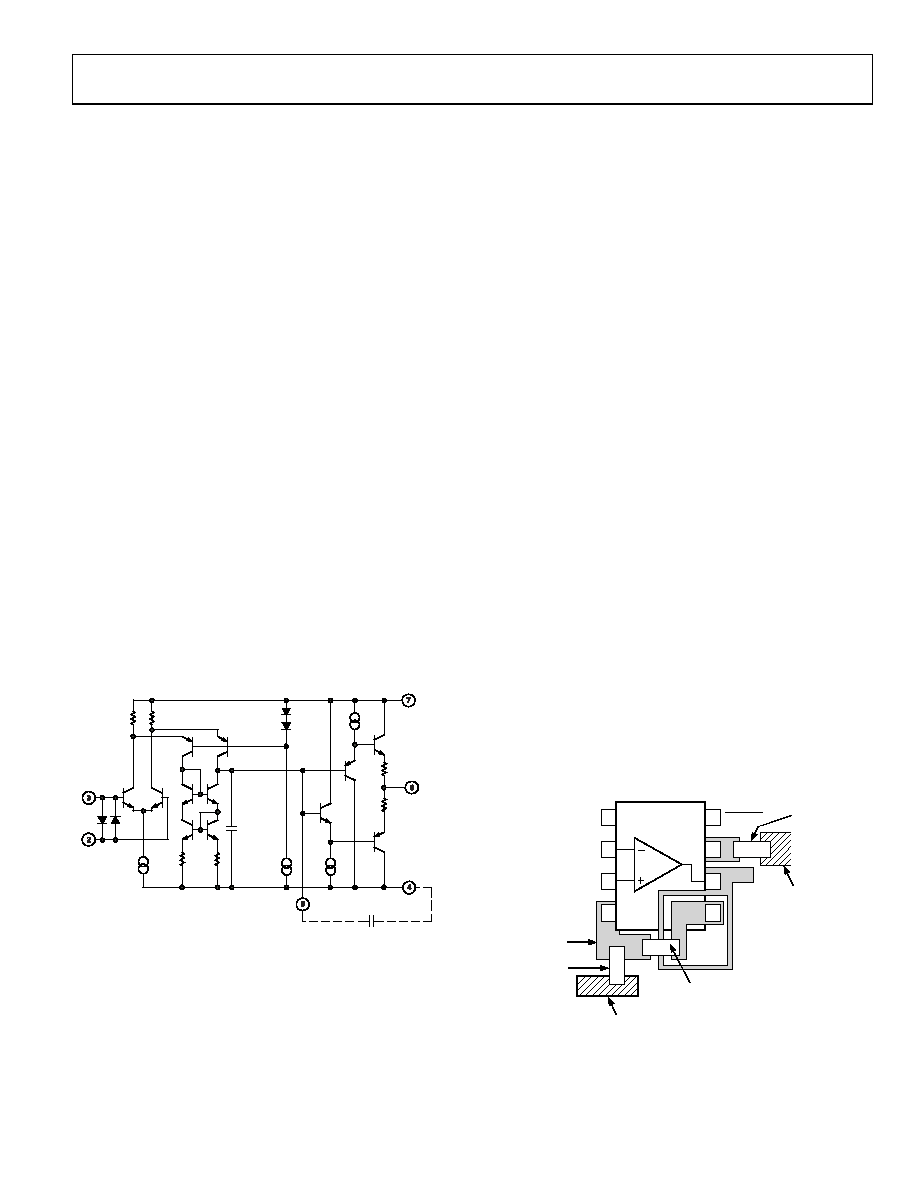
As shown in Figure 61, the AD8021 input stage consists of an
NPN differential pair in which each transistor operates at a
0.8 mA collector current. This allows the input devices a high
transconductance; thus, the AD8021 has a low input noise of
2.1 nV/√Hz @ 50 kHz. The input stage drives a folded cascode
that consists of a pair of PNP transistors. The folded cascode
and current mirror provide a differential-to-single-ended
conversion of signal current. This current then drives the high
impedance node (Pin 5), where the CC external capacitor is
connected. The output stage preserves this high impedance with
a current gain of 5000, so that the AD8021 can maintain a high
open-loop gain even when driving heavy loads.
Two internal diode clamps across the inputs (Pin 2 and Pin 3)
protect the input transistors from large voltages that could
otherwise cause emitter-base breakdown, which would result in
degradation of offset voltage and input bias current.
+IN
–IN
CINTERNAL
1.5pF
CCOMP
CC
–VS
+VS
OUTPUT
01888-061
Figure 61. Simplified Schematic
PCB LAYOUT CONSIDERATIONS
As with all high speed op amps, achieving optimum performance
from the AD8021 requires careful attention to PC board layout.
Particular care must be exercised to minimize lead lengths
between the ground leads of the bypass capacitors and between
the compensation capacitor and the negative supply. Otherwise,
lead inductance can influence the frequency response and even
cause high frequency oscillations. Use of a multilayer printed
circuit board, with an internal ground plane, reduces ground
noise and enables a compact component arrangement.
Due to the relatively high impedance of Pin 5 and low values of
the compensation capacitor, a guard ring is recommended. The
guard ring is simply a PC trace that encircles Pin 5 and is
connected to the output, Pin 6, which is at the same potential as
Pin 5. This serves two functions. It shields Pin 5 from any local
circuit noise generated by surrounding circuitry. It also
minimizes stray capacitance, which would tend to otherwise
reduce the bandwidth. An example of a guard ring layout is
shown in Figure 62.
Also shown in Figure 62, the compensation capacitor is located
immediately adjacent to the edge of the AD8021 package, spanning
Pin 4 and Pin 5. This capacitor must be a high quality surface-
mount COG or NPO ceramic. The use of leaded capacitors is
not recommended. The high frequency bypass capacitor(s)
should be located immediately adjacent to the supplies,
Pin 4 and Pin 7.
To achieve the shortest possible lead length at the inverting
input, the feedback resistor RF is located beneath the board and
spans the distance from the output, Pin 6, to inverting input
Pin 2. The return node of Resistor RG should be situated as close
as possible to the return node of the negative supply bypass
capacitor connected to Pin 4.
DISABLE
VOUT
8
7
6
1
2
3
LOGIC REFERENCE
–IN
+IN
–VS 4
+VS
5
CCOMP
GROUND
PLANE
BYPASS
CAPACITOR
COMPENSATION
CAPACITOR
GROUND
PLANE
BYPASS
CAPACITOR
METAL
(TOP VIEW)
01888-062
Figure 62. Recommended Location of
Critical Components and Guard Ring
相关PDF资料 |
PDF描述 |
|---|---|
| TMM-116-01-G-S-SM | CONN HEADER 16POS SNGL 2MM SMD |
| LTC6101HVAHMS8#TRPBF | IC AMP CURRENT SENSE 8-MSOP |
| TSW-133-23-S-S | CONN HEADER 33POS .100" SGL GOLD |
| TSW-119-23-G-D | CONN HEADER 38POS .100" DL GOLD |
| LTC6253CMS#TRPBF | IC OPAMP R-R 720MHZ MSOP-10 |
相关代理商/技术参数 |
参数描述 |
|---|---|
| AD8021ARM-REEL | 功能描述:IC OPAMP VF LN LP LDIST 8MSOP RoHS:否 类别:集成电路 (IC) >> Linear - Amplifiers - Instrumentation 系列:- 标准包装:1,000 系列:- 放大器类型:电压反馈 电路数:4 输出类型:满摆幅 转换速率:33 V/µs 增益带宽积:20MHz -3db带宽:30MHz 电流 - 输入偏压:2nA 电压 - 输入偏移:3000µV 电流 - 电源:2.5mA 电流 - 输出 / 通道:30mA 电压 - 电源,单路/双路(±):4.5 V ~ 16.5 V,±2.25 V ~ 8.25 V 工作温度:-40°C ~ 85°C 安装类型:表面贴装 封装/外壳:14-SOIC(0.154",3.90mm 宽) 供应商设备封装:14-SOIC 包装:带卷 (TR) |
| AD8021ARM-REEL7 | 功能描述:IC OPAMP VF LN LP LDIST 8MSOP RoHS:否 类别:集成电路 (IC) >> Linear - Amplifiers - Instrumentation 系列:- 标准包装:50 系列:- 放大器类型:通用 电路数:2 输出类型:满摆幅 转换速率:1.8 V/µs 增益带宽积:6.5MHz -3db带宽:4.5MHz 电流 - 输入偏压:5nA 电压 - 输入偏移:100µV 电流 - 电源:65µA 电流 - 输出 / 通道:35mA 电压 - 电源,单路/双路(±):1.8 V ~ 5.25 V,±0.9 V ~ 2.625 V 工作温度:-40°C ~ 85°C 安装类型:表面贴装 封装/外壳:10-TFSOP,10-MSOP(0.118",3.00mm 宽) 供应商设备封装:10-MSOP 包装:管件 |
| AD8021ARMZ | 功能描述:IC OPAMP VF LN LP LDIST 8MSOP RoHS:是 类别:集成电路 (IC) >> Linear - Amplifiers - Instrumentation 系列:- 产品培训模块:Differential Circuit Design Techniques for Communication Applications 标准包装:1 系列:- 放大器类型:RF/IF 差分 电路数:1 输出类型:差分 转换速率:9800 V/µs 增益带宽积:- -3db带宽:2.9GHz 电流 - 输入偏压:3µA 电压 - 输入偏移:- 电流 - 电源:40mA 电流 - 输出 / 通道:- 电压 - 电源,单路/双路(±):3 V ~ 3.6 V 工作温度:-40°C ~ 85°C 安装类型:表面贴装 封装/外壳:16-VQFN 裸露焊盘,CSP 供应商设备封装:16-LFCSP-VQ 包装:剪切带 (CT) 产品目录页面:551 (CN2011-ZH PDF) 其它名称:ADL5561ACPZ-R7CT |
| AD8021ARMZ-REEL | 功能描述:IC OPAMP VF LN LP LDIST 8MSOP RoHS:是 类别:集成电路 (IC) >> Linear - Amplifiers - Instrumentation 系列:- 标准包装:1,000 系列:- 放大器类型:电压反馈 电路数:4 输出类型:满摆幅 转换速率:33 V/µs 增益带宽积:20MHz -3db带宽:30MHz 电流 - 输入偏压:2nA 电压 - 输入偏移:3000µV 电流 - 电源:2.5mA 电流 - 输出 / 通道:30mA 电压 - 电源,单路/双路(±):4.5 V ~ 16.5 V,±2.25 V ~ 8.25 V 工作温度:-40°C ~ 85°C 安装类型:表面贴装 封装/外壳:14-SOIC(0.154",3.90mm 宽) 供应商设备封装:14-SOIC 包装:带卷 (TR) |
| AD8021ARMZ-REEL7 | 功能描述:IC OPAMP VF LN LP LDIST 8MSOP RoHS:是 类别:集成电路 (IC) >> Linear - Amplifiers - Instrumentation 系列:- 标准包装:1,000 系列:- 放大器类型:电压反馈 电路数:4 输出类型:满摆幅 转换速率:33 V/µs 增益带宽积:20MHz -3db带宽:30MHz 电流 - 输入偏压:2nA 电压 - 输入偏移:3000µV 电流 - 电源:2.5mA 电流 - 输出 / 通道:30mA 电压 - 电源,单路/双路(±):4.5 V ~ 16.5 V,±2.25 V ~ 8.25 V 工作温度:-40°C ~ 85°C 安装类型:表面贴装 封装/外壳:14-SOIC(0.154",3.90mm 宽) 供应商设备封装:14-SOIC 包装:带卷 (TR) |
发布紧急采购,3分钟左右您将得到回复。