参数资料
| 型号: | AD8030AR |
| 厂商: | Analog Devices Inc |
| 文件页数: | 10/25页 |
| 文件大小: | 0K |
| 描述: | IC AMP GP R-R DUAL LP 8SOIC |
| 标准包装: | 98 |
| 放大器类型: | 通用 |
| 电路数: | 2 |
| 输出类型: | 满摆幅 |
| 转换速率: | 63 V/µs |
| -3db带宽: | 125MHz |
| 电流 - 输入偏压: | 1.7µA |
| 电压 - 输入偏移: | 2000µV |
| 电流 - 电源: | 1.4mA |
| 电流 - 输出 / 通道: | 170mA |
| 电压 - 电源,单路/双路(±): | 2.7 V ~ 12 V,±1.35 V ~ 6 V |
| 工作温度: | -40°C ~ 125°C |
| 安装类型: | 表面贴装 |
| 封装/外壳: | 8-SOIC(0.154",3.90mm 宽) |
| 供应商设备封装: | 8-SO |
| 包装: | 管件 |
Data Sheet
AD8029/AD8030/AD8040
Rev. B | Page 17 of 24
APPLICATIONS
WIDEBAND OPERATION
+VS
–VS
C2
10
F
C1
0.1
F
C4
0.1
F
C3
10
F
VOUT
+
–
AD8029
RG
R1
RF
DISABLE
VIN
R1 = RF||RG
03679-0-052
Figure 51. Wideband Non-inverting Gain Configuration
+VS
–VS
C1
0.1
F
C4
0.1
F
C3
10
F
R1
VOUT
–
+
AD8029
RG
R1 = RF||RG
RF
VIN
03679-0-053
C2
10
F
DISABLE
Figure 52. Wideband Inverting Gain Configuration
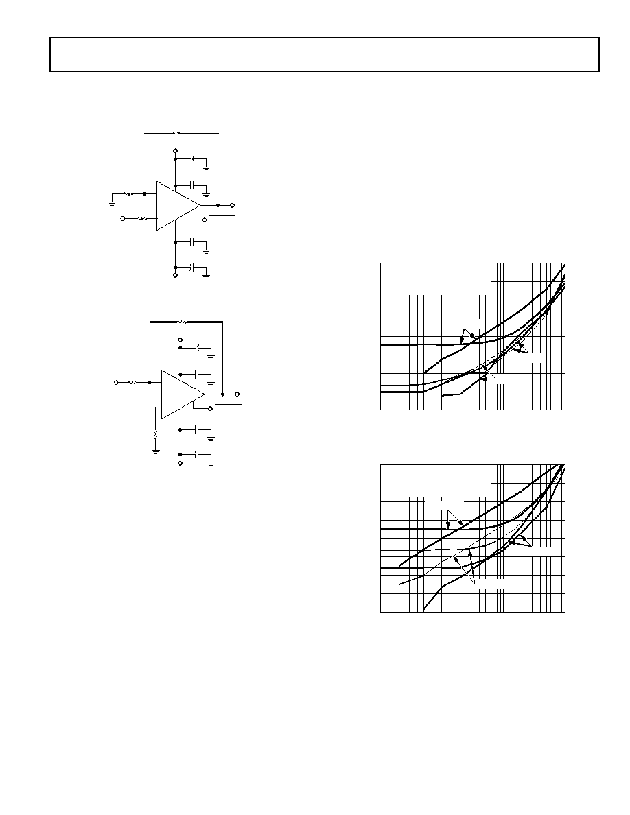
OUTPUT LOADING SENSITIVITY
To achieve maximum performance and low power dissipation,
the designer needs to consider the loading at the output of
AD8029/AD8030/AD8040. Table 5 shows the effects of output
loading and performance.
When operating at unity gain, the effective load at the amplifier
output is the resistance (RL) being driven by the amplifier. For
gains other than 1, in noninverting configurations, the feedback
network represents an additional current load at the amplifier
output. The feedback network (RF + RG) is in parallel with RL,
which lowers the effective resistance at the output of the
amplifier. The lower effective resistance causes the amplifier to
supply more current at the output. Lower values of feedback
resistance increase the current draw, thus increasing the
amplifier’s power dissipation.
For example, if using the values shown in Table 5 for a gain of 2,
with resistor values of 2.5 k, the effective load at the output is
1.67 k. For inverting configurations, only the feedback resistor
RF is in parallel with the output load. If the load is greater than
that specified in the data sheet, the amplifier can introduce
nonlinearities in its open-loop response, which increases
distortion. Figure 53 and Figure 54 illustrate effective output
loading and distortion performance. Increasing the resistance of
the feedback network can reduce the current consumption, but
has other implications.
FREQUENCY (MHz)
HARMONIC
DISTORTION
(dBc)
0.01
–120
0.1
1.0
10
03679-A-008
–40
–50
–60
–70
–80
–90
–100
–110
VS = 5V
VOUT = 0.1V p-p
RL = 5k
RL = 2.5k
VS = 5V
VOUT = 2.0V p-p
SECOND HARMONIC – SOLID LINES
THIRD HARMONIC – DOTTED LINES
RL = 1k
Figure 53. Gain of 1 Distortion
FREQUENCY (MHz)
HARMONIC
DISTORTION
(dBc)
0.01
–120
0.1
1.0
10
03679-A-009
–40
–50
–60
–70
–80
–90
–100
–110
VS = 5V
VOUT = 0.1V p-p
RF = RL = 1k
VS = 5V
VOUT = 2.0V p-p
SECOND HARMONIC – SOLID LINES
THIRD HARMONIC – DOTTED LINES
RF = RL = 5k
RF = RL = 2.5k
Figure 54. Gain of 2 Distortion
相关PDF资料 |
PDF描述 |
|---|---|
| TSW-149-08-G-S | CONN HEADER 49POS .100" SGL GOLD |
| 929550-01-30-EU | CONN HEADER .100 SNGL R/A 30POS |
| 9-103325-0-34 | CONN HEADR BRKWAY .100 34POS R/A |
| AS168X-CB1DG100N-613 | CIRCUIT BRKR THERMAL 10A 1POLE |
| GBC29SFBN-M30 | CONN HEADER 29PS .100 SINGLE SMD |
相关代理商/技术参数 |
参数描述 |
|---|---|
| AD8030AR | 制造商:Analog Devices 功能描述:AMP LOW POWER RRI/O 8030 SOIC8 |
| AD8030AR-EBZ | 功能描述:BOARD EVAL FOR AD8030AR RoHS:是 类别:编程器,开发系统 >> 评估板 - 运算放大器 系列:- 产品培训模块:Lead (SnPb) Finish for COTS Obsolescence Mitigation Program 标准包装:1 系列:- |
| AD8030ARJ | 制造商:Analog Devices 功能描述:OP AMP DUAL GP R-R I/O 6V/12V 8PIN SOT-23 - Bulk |
| AD8030ARJ-EBZ | 功能描述:BOARD EVAL FOR AD8030ARJ RoHS:是 类别:编程器,开发系统 >> 评估板 - 运算放大器 系列:- 产品培训模块:Lead (SnPb) Finish for COTS Obsolescence Mitigation Program 标准包装:1 系列:- |
| AD8030ARJ-R2 | 制造商:Analog Devices 功能描述:OP Amp Dual GP R-R I/O ±6V/12V 8-Pin SOT-23 T/R 制造商:Rochester Electronics LLC 功能描述:LOW POWER R-R I/O AMP - Bulk |
发布紧急采购,3分钟左右您将得到回复。