参数资料
| 型号: | AD8037ARZ |
| 厂商: | Analog Devices Inc |
| 文件页数: | 14/24页 |
| 文件大小: | 0K |
| 描述: | IC OPAMP VF ULDIST LN 70MA 8SOIC |
| 标准包装: | 98 |
| 系列: | CLAMPIN™ |
| 放大器类型: | 电压反馈 |
| 电路数: | 1 |
| 转换速率: | 1500 V/µs |
| -3db带宽: | 270MHz |
| 电流 - 输入偏压: | 3µA |
| 电压 - 输入偏移: | 2000µV |
| 电流 - 电源: | 18.5mA |
| 电流 - 输出 / 通道: | 70mA |
| 电压 - 电源,单路/双路(±): | ±3 V ~ 6 V |
| 工作温度: | -40°C ~ 85°C |
| 安装类型: | 表面贴装 |
| 封装/外壳: | 8-SOIC(0.154",3.90mm 宽) |
| 供应商设备封装: | 8-SOIC |
| 包装: | 管件 |
| 产品目录页面: | 769 (CN2011-ZH PDF) |
| 配用: | AD8037-EB-ND - BOARD EVAL FOR AD8037 |
REV. B
–20–
AD8036/AD8037
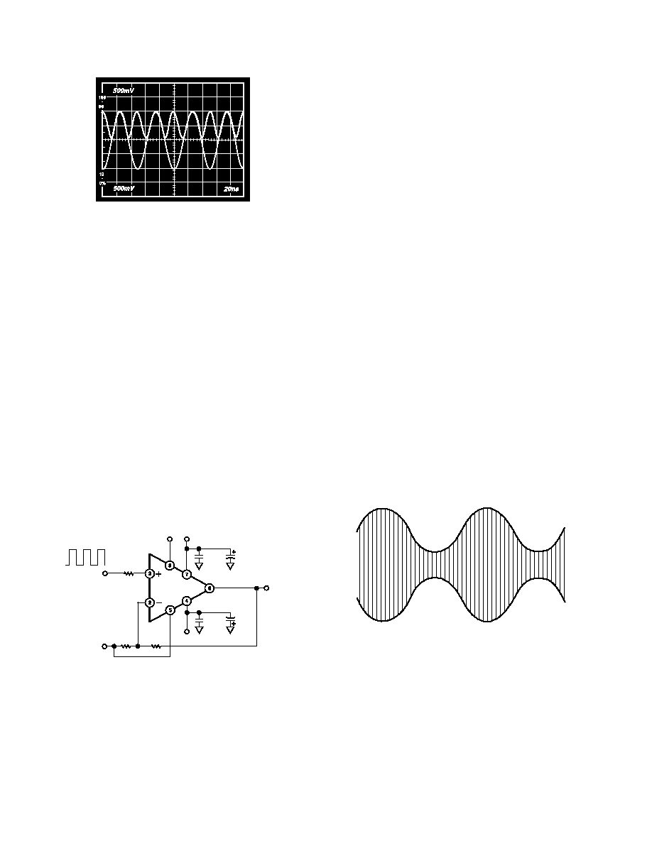
Figure 14. Full-Wave Rectifier Scope
Thus for either positive or negative input signals, the output is
unity times the absolute value of the input signal. The circuit
can be easily configured to produce the negative absolute value
of the input by applying the input to VH instead of VL.
The circuit can get to within about 40 mV of ground during the
time when the input crosses zero. This voltage is fixed over a
wide frequency range and is a result of the switching between
the conventional op amp input and the clamp input. But because
there are no diodes to rapidly switch from forward to reverse bias,
the performance far exceeds that of diode based full wave rectifiers.
The 40 mV offset mentioned can be removed by adding an off-
set to the circuit. A 27.4 k
input resistor to the inverting input
will have a gain of 0.01, while changing the gain of the circuit
by only 1%. A plus or minus 4 V dc level (depending on the
polarity of the rectifier) into this resistor will compensate for
the offset.
Full wave rectifiers are useful in many applications including
AM signal detection, high frequency ac voltmeters and various
arithmetic operations.
Amplitude Modulator
In addition to being able to be configured as an amplitude
demodulator (AM detector), the AD8037 can also be config-
ured as an amplitude modulator as shown in Figure 15.
CARRIER IN
VH
AM OUT
MODULATION IN
+5V
RF
274
–5V
100
VH
VL
0.1 F10 F
AD8037
0.1 F
10 F
RG
274
Figure 15. Amplitude Modulator
The positive input of the AD8037 is driven with a square wave
of sufficient amplitude to produce clamping action at both the
high and low levels. This is the higher frequency carrier signal.
The modulation signal is applied to both the input of a unity
gain inverting amplifier and to VL, the lower clamping input.
VH is biased at 0.5 V dc.
To understand the circuit operation, it is helpful to first con-
sider a simpler circuit. If both VL and VH were dc biased at
–0.5 V and the carrier and modulation inputs driven as above,
the output would be a 2 V p-p square wave at the carrier fre-
quency riding on a waveform at the modulating frequency. The
inverting input (modulation signal) is creating a varying offset to
the 2 V p-p square wave at the output. Both the high and low
levels clamp at twice the input levels on the clamps because the
noise gain of the circuit is two.
When VL is driven by the modulation signal instead of being held
at a dc level, a more complicated situation results. The resulting
waveform is composed of an upper envelope and a lower enve-
lope with the carrier square wave in between. The upper and
lower envelope waveforms are 180
° out of phase as in a typical
AM waveform.
The upper envelope is produced by the upper clamp level being
offset by the waveform applied to the inverting input. This offset
is the opposite polarity of the input waveform because of the
inverting configuration.
The lower envelope is produced by the sum of two effects. First,
it is offset by the waveform applied to the inverting input as in
the case of the simplified circuit above. The polarity of this off-
set is in the same direction as the upper envelope. Second, the
output is driven in the opposite direction of the offset at twice
the offset voltage by the modulation signal being applied to VL.
This results from the noise gain being equal to two, and since
there is no inversion in this connection, it is opposite polarity
from the offset.
The result at the output for the lower envelope is the sum of
these two effects, which produces the lower envelope of an
amplitude modulated waveform. See Figure 16.
Figure 16. AM Waveform
The depth of modulation can be modified in this circuit by
changing the amplitude of the modulation signal. This changes
the amplitude of the upper and lower envelope waveforms.
The modulation depth can also be changed by changing the dc
bias applied to VH. In this case the amplitudes of the upper and
lower envelope waveforms stay constant, but the spacing between
them changes. This alters the ratio of the envelope amplitude to
the amplitude of the overall waveform.
相关PDF资料 |
PDF描述 |
|---|---|
| TSW-112-08-G-S-RA | CONN HEADER 12PS .100 SGL R/A AU |
| TSW-113-08-G-S | CONN HEADER 13POS .100" SGL GOLD |
| PEC20SBBN | CONN HEADER .100 SINGL R/A 20POS |
| PBC11SFCN | CONN HEADER .100 SINGL STR 11POS |
| PEC08DFBN | CONN HEADER .100 DUAL STR 16POS |
相关代理商/技术参数 |
参数描述 |
|---|---|
| AD8037ARZ-REEL | 功能描述:IC OPAMP VF ULDIST LN 70MA 8SOIC RoHS:是 类别:集成电路 (IC) >> Linear - Amplifiers - Instrumentation 系列:CLAMPIN™ 标准包装:50 系列:- 放大器类型:J-FET 电路数:2 输出类型:- 转换速率:3.5 V/µs 增益带宽积:1MHz -3db带宽:- 电流 - 输入偏压:30pA 电压 - 输入偏移:2000µV 电流 - 电源:200µA 电流 - 输出 / 通道:- 电压 - 电源,单路/双路(±):7 V ~ 36 V,±3.5 V ~ 18 V 工作温度:0°C ~ 70°C 安装类型:通孔 封装/外壳:8-DIP(0.300",7.62mm) 供应商设备封装:8-PDIP 包装:管件 |
| AD8037ARZ-REEL7 | 功能描述:IC OPAMP VF ULDIST LN 70MA 8SOIC RoHS:是 类别:集成电路 (IC) >> Linear - Amplifiers - Instrumentation 系列:CLAMPIN™ 标准包装:150 系列:- 放大器类型:音频 电路数:2 输出类型:- 转换速率:5 V/µs 增益带宽积:12MHz -3db带宽:- 电流 - 输入偏压:100nA 电压 - 输入偏移:500µV 电流 - 电源:6mA 电流 - 输出 / 通道:50mA 电压 - 电源,单路/双路(±):4 V ~ 32 V,±2 V ~ 16 V 工作温度:-40°C ~ 85°C 安装类型:表面贴装 封装/外壳:8-TSSOP(0.173",4.40mm 宽) 供应商设备封装:8-TSSOP 包装:管件 |
| AD8037-EB | 功能描述:BOARD EVAL FOR AD8037 RoHS:否 类别:编程器,开发系统 >> 评估板 - 运算放大器 系列:- 产品培训模块:Lead (SnPb) Finish for COTS Obsolescence Mitigation Program 标准包装:1 系列:- |
| AD8037SRZ-EP | 功能描述:IC OPAMP VF LP LN LDIST 8SOIC 制造商:analog devices inc. 系列:- 包装:管件 零件状态:在售 放大器类型:电压反馈 电路数:1 输出类型:- 压摆率:1500 V/μs -3db 带宽:270MHz 电流 - 输入偏置:3μA 电压 - 输入失调:2mV 电流 - 电源:18.5mA 电流 - 输出/通道:70mA 电压 - 电源,单/双(±):±3 V ~ 6 V 工作温度:-55°C ~ 105°C 安装类型:表面贴装 封装/外壳:8-SOIC(0.154",3.90mm 宽) 供应商器件封装:8-SOIC 标准包装:1 |
| AD8037SRZ-EP-R7 | 功能描述:Voltage Feedback Amplifier 1 Circuit 8-SOIC 制造商:analog devices inc. 系列:- 包装:带卷(TR) 零件状态:有效 放大器类型:电压反馈 电路数:1 输出类型:- 压摆率:1500 V/μs 增益带宽积:- -3db 带宽:270MHz 电流 - 输入偏置:3μA 电压 - 输入失调:2mV 电流 - 电源:18.5mA 电流 - 输出/通道:70mA 电压 - 电源,单/双(±):±3 V ~ 6 V 工作温度:-55°C ~ 105°C 安装类型:表面贴装 封装/外壳:8-SOIC(0.154",3.90mm 宽) 供应商器件封装:8-SOIC 标准包装:1,000 |
发布紧急采购,3分钟左右您将得到回复。