参数资料
| 型号: | AD8038ARZ |
| 厂商: | Analog Devices Inc |
| 文件页数: | 14/17页 |
| 文件大小: | 0K |
| 描述: | IC OPAMP VF LP LN LDIST 8SOIC |
| 设计资源: | AC Signal Processing Using AD5426/32/43 Current Output DACs (CN0037) AC Signal Processing Using AD5450/1/2/3 Current Output DACs (CN0054) |
| 标准包装: | 98 |
| 放大器类型: | 电压反馈 |
| 电路数: | 1 |
| 转换速率: | 425 V/µs |
| -3db带宽: | 350MHz |
| 电流 - 输入偏压: | 400pA |
| 电压 - 输入偏移: | 500µV |
| 电流 - 电源: | 1mA |
| 电压 - 电源,单路/双路(±): | 3 V ~ 12 V,±1.5 V ~ 6 V |
| 工作温度: | -40°C ~ 85°C |
| 安装类型: | 表面贴装 |
| 封装/外壳: | 8-SOIC(0.154",3.90mm 宽) |
| 供应商设备封装: | 8-SO |
| 包装: | 管件 |
| 产品目录页面: | 769 (CN2011-ZH PDF) |
AD8038/AD8039
Rev. G | Page 5 of 16
ABSOLUTE MAXIMUM RATINGS
Table 3.
Parameter
Rating
Supply Voltage
12.6 V
Power Dissipation
See Figure 5
Common-Mode Input Voltage
±VS
Differential Input Voltage
±4 V
Storage Temperature Range
65°C to +125°C
Operating Temperature Range
40°C to +85°C
Lead Temperature (Soldering, 10 sec)
300°C
Stresses above those listed under Absolute Maximum Ratings
may cause permanent damage to the device. This is a stress
rating only; functional operation of the device at these or any
other conditions above those indicated in the operational
section of this specification is not implied. Exposure to absolute
maximum rating conditions for extended periods may affect
device reliability.
MAXIMUM POWER DISSIPATION
The maximum safe power dissipation in the AD8038/AD8039
package is limited by the associated rise in junction temperature
(TJ) on the die. The plastic encapsulating the die locally reaches
the junction temperature. At approximately 150°C, which is the
glass transition temperature, the plastic changes its properties.
Even temporarily exceeding this temperature limit may change
the stresses that the package exerts on the die, permanently
shifting the parametric performance of the AD8038/AD8039.
Exceeding a junction temperature of 175°C for an extended
time can result in changes in the silicon devices, potentially
causing failure.
The still-air thermal properties of the package and PCB (θJA),
ambient temperature (TA), and total power dissipated in the
package (PD) determine the junction temperature of the die.
The junction temperature can be calculated as
TJ = TA + (PD × θJA)
The power dissipated in the package (PD) is the sum of the
quiescent power dissipation and the power dissipated in the
package due to the load drive for all outputs. The quiescent power
is the voltage between the supply pins (VS) multiplied by the
quiescent current (IS). Assuming the load (RL) is referenced to
midsupply, then the total drive power is VS/2 × IOUT, some of which
is dissipated in the package and some in the load (VOUT × IOUT).
The difference between the total drive power and the load
power is the drive power dissipated in the package.
PD = quiescent power + (total drive power load power)
PD = [VS × IS] + [(VS/2) × (VOUT/RL)] [VOUT2/RL]
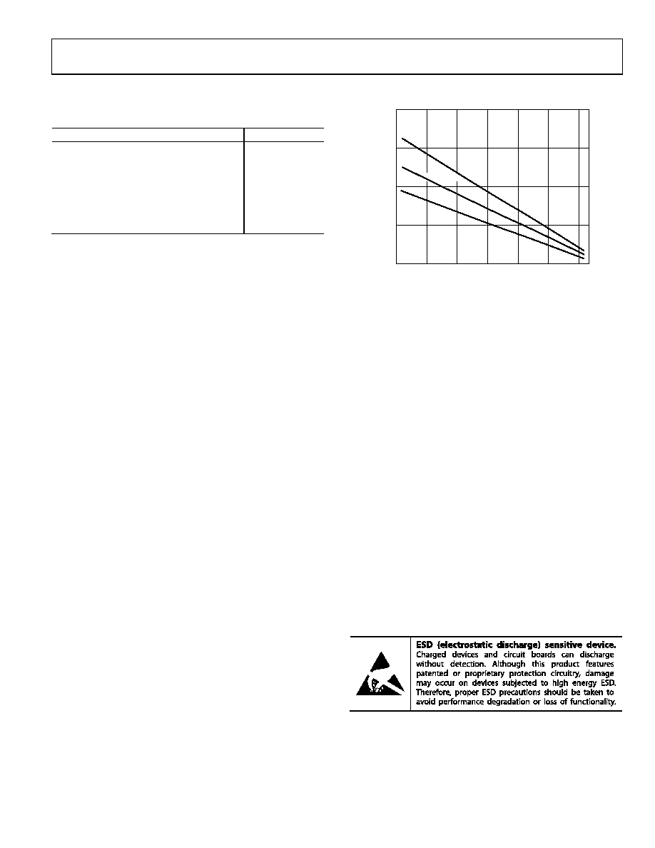
AMBIENT TEMPERATURE (°C)
0
–55
MA
XI
MU
M
P
O
W
E
R
D
IS
S
IPA
T
IO
N
(W
)
1.0
–25
5
35
65
95
125
1.5
2.0
SOIC-8
0.5
SC70-5
SOT-23-8
02
95
1-
00
5
Figure 5. Maximum Power Dissipation vs. Temperature for a 4-Layer Board
RMS output voltages should be considered. If RL is referenced to
VS, as in single-supply operation, then the total drive power is
VS × IOUT. If the rms signal levels are indeterminate, consider the
worst case, when VOUT = VS /4 for RL to midsupply
PD = (VS × IS) + (VS/4)2/RL
In single-supply operation with RL referenced to VS, worst case
is VOUT = VS /2.
Airflow increases heat dissipation, effectively reducing θJA. In
addition, more metal directly in contact with the package leads
from metal traces, throughholes, ground, and power planes reduce
the θJA. Care must be taken to minimize parasitic capacitances at
the input leads of high speed op amps as discussed in the
Figure 5 shows the maximum safe power dissipation in the
package vs. the ambient temperature for the 8-lead SOIC
(125°C/W), 5-lead SC70 (210°C/W), and 8-lead SOT-23
(160°C/W) packages on a JEDEC standard 4-layer board.
θJA values are approximations.
OUTPUT SHORT CIRCUIT
Shorting the output to ground or drawing excessive current
from the AD8038/AD8039 will likely cause a catastrophic failure.
ESD CAUTION
相关PDF资料 |
PDF描述 |
|---|---|
| AD8063ARZ | IC OPAMP VF R-R LP 50MA 8SOIC |
| AD8051ARZ | IC OPAMP VF R-R LDIST LP 8SOIC |
| TSW-116-23-T-S | CONN HEADER 16POS .100" SNGL TIN |
| ADA4899-1YCPZ-R7 | IC OPAMP VF ULN ULDIST 8LFCSP |
| 929647-01-02-I | CONN HEADER 2POS STR .100 GOLD |
相关代理商/技术参数 |
参数描述 |
|---|---|
| AD8038ARZ | 制造商:Analog Devices 功能描述:IC OP-AMP 350MHZ 425V/S SOIC-8 |
| AD8038ARZ-REEL | 功能描述:IC OPAMP VF LP LN LDIST 8SOIC RoHS:是 类别:集成电路 (IC) >> Linear - Amplifiers - Instrumentation 系列:- 标准包装:160 系列:- 放大器类型:通用 电路数:4 输出类型:满摆幅 转换速率:10 V/µs 增益带宽积:9MHz -3db带宽:- 电流 - 输入偏压:1pA 电压 - 输入偏移:250µV 电流 - 电源:730µA 电流 - 输出 / 通道:28mA 电压 - 电源,单路/双路(±):2.7 V ~ 5.5 V,±1.35 V ~ 2.75 V 工作温度:-40°C ~ 125°C 安装类型:表面贴装 封装/外壳:16-SOIC(0.154",3.90mm 宽) 供应商设备封装:16-SOIC N 包装:管件 |
| AD8038ARZ-REEL7 | 功能描述:IC OPAMP VF LP LN LDIST 8SOIC RoHS:是 类别:集成电路 (IC) >> Linear - Amplifiers - Instrumentation 系列:- 标准包装:2,500 系列:- 放大器类型:通用 电路数:1 输出类型:满摆幅 转换速率:0.11 V/µs 增益带宽积:350kHz -3db带宽:- 电流 - 输入偏压:4nA 电压 - 输入偏移:20µV 电流 - 电源:260µA 电流 - 输出 / 通道:20mA 电压 - 电源,单路/双路(±):2.7 V ~ 36 V,±1.35 V ~ 18 V 工作温度:-40°C ~ 85°C 安装类型:表面贴装 封装/外壳:8-SOIC(0.154",3.90mm 宽) 供应商设备封装:8-SO 包装:带卷 (TR) |
| AD8039 | 制造商:AD 制造商全称:Analog Devices 功能描述:Low Power 350 MHz Voltage Feedback Amplifiers |
| AD-8039 | 制造商:BOTHHAND 制造商全称:Bothhand USA, LP. 功能描述:ADSL CPE SIDE SPLITTER |
发布紧急采购,3分钟左右您将得到回复。