参数资料
| 型号: | AD8042AN |
| 厂商: | Analog Devices Inc |
| 文件页数: | 5/17页 |
| 文件大小: | 0K |
| 描述: | IC OPAMP VF R-R DUAL LP 8DIP |
| 设计资源: | Single-Ended-to-Differential Converters for Voltage Output and Current Output DACs Using AD8042 (CN0143) |
| 标准包装: | 50 |
| 放大器类型: | 电压反馈 |
| 电路数: | 2 |
| 输出类型: | 满摆幅 |
| 转换速率: | 225 V/µs |
| -3db带宽: | 170MHz |
| 电流 - 输入偏压: | 1.2µA |
| 电压 - 输入偏移: | 3000µV |
| 电流 - 电源: | 6mA |
| 电流 - 输出 / 通道: | 50mA |
| 电压 - 电源,单路/双路(±): | 3 V ~ 12 V,±1.5 V ~ 6 V |
| 工作温度: | -40°C ~ 85°C |
| 安装类型: | 通孔 |
| 封装/外壳: | 8-DIP(0.300",7.62mm) |
| 供应商设备封装: | 8-PDIP |
| 包装: | 管件 |
AD8042
Rev. E | Page 12 of 16
APPLICATIONS INFORMATION
CIRCUIT DESCRIPTION
The AD8042 is fabricated on the Analog Devices, Inc.,
proprietary eXtra-Fast Complementary Bipolar (XFCB)
process, which enables the construction of PNP and NPN
transistors with similar fts in the 2 GHz to 4 GHz region. The
process is dielectrically isolated to eliminate the parasitic and
latch-up problems caused by junction isolation. These features
allow the construction of high frequency, low distortion
amplifiers with low supply currents. This design uses a
differential output input stage to maximize bandwidth and
headroom (see Figure 35). The smaller signal swings required
on the first stage outputs (nodes SIP, SIN) reduce the effect of
nonlinear currents due to junction capacitances and improve
the distortion performance. With this design, harmonic distortion
of better than 77 dB @ 1 MHz into 100 Ω with VOUT = 2 V p-p
(gain = +2) on a single 5 V supply is achieved.
01059-
036
SIN
R21
R3
VEE
Q11
Q3
I10
R26
R39
Q5
Q4
Q40
I7
R2
R15
Q13
Q17
R5
C7
Q2
SIP
Q22
Q7
Q21
Q24
R23 R27
I2
I3
I1
Q51
Q25
Q50
Q39
Q47
Q27
Q31
Q23
I9
I5
VEE
VCC
I8
Q36
Q8
VOUT
C3
C9
VCC
VINP
VINN
VEE
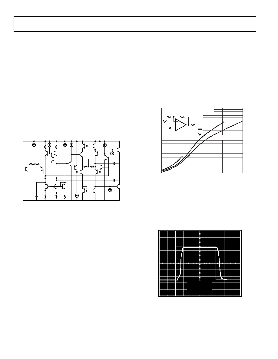
Figure 35. Simplified Schematic
The rail-to-rail output range of the AD8042 is provided by a
complementary common-emitter output stage. High output
drive capability is provided by injecting all output stage predriver
currents directly into the bases of the output devices Q8 and
Q36. Biasing of Q8 and Q36 is accomplished by I8 and I5, along
with a common-mode feedback loop (not shown). This circuit
topology allows the AD8042 to drive 40 mA of output current
with the outputs within 0.5 V of the supply rails.
On the input side, the device can handle voltages from 0.2 V
below the negative rail to within 1.2 V of the positive rail.
Exceeding these values does not cause phase reversal; however,
the input ESD devices do begin to conduct if the input voltages
exceed the rails by greater than 0.5 V.
DRIVING CAPACITIVE LOADS
The capacitive load drive of the AD8042 can be increased by
adding a low valued resistor in series with the load. Figure 36
shows the effects of a series resistor on capacitive drive for
varying voltage gains. As the closed-loop gain is increased, the
larger phase margin allows for larger capacitive loads with less
overshoot. Adding a series resistor with lower closed-loop gains
accomplishes the same effect. For large capacitive loads, the
frequency response of the amplifier is dominated by the roll-off
of the series resistor and capacitive load.
1000
100
10
15
24
3
CAP
ACI
T
IV
E
L
O
A
D
(
p
F
)
CLOSED-LOOP GAIN (V/V)
01
05
9-
03
7
CL
RS
VS = 5V
200mV STEP WITH 90% OVERSHOOT
RS = 20
RS = 5
RS = 0
Figure 36. Capacitive Load Drive vs. Closed-Loop Gain
OVERDRIVE RECOVERY
Overdrive of an amplifier occurs when the output and/or input
range are exceeded. The amplifier must recover from this overdrive
condition. As shown in Figure 37, the AD8042 recovers within
30 ns from negative overdrive and within 25 ns from positive
overdrive.
5.0V
2.5V
0V
0
10
59
-03
5
G = +2
VS = 5V
VIN = 5V p-p
RL = 1k TO 2.5V
50ns
1V
Figure 37. Overdrive Recovery
相关PDF资料 |
PDF描述 |
|---|---|
| Y16361K00000T9W | RES 1K OHM .1W .01% FOIL 0603 |
| Y16070R50000F9W | RES .5 OHM .5W 1% FOIL SMD |
| TMM-144-01-S-S-SM | CONN HEADER 44POS SNGL 2MM SMD |
| LT1228CS8 | IC CURRNT FEEDBK AMP 100MHZ8SOIC |
| 170M3415 | FUSE 200A 690V 1BN/50 AR UC |
相关代理商/技术参数 |
参数描述 |
|---|---|
| AD8042AR | 功能描述:IC OPAMP VF R-R DUAL LP 8SOIC RoHS:否 类别:集成电路 (IC) >> Linear - Amplifiers - Instrumentation 系列:- 标准包装:50 系列:- 放大器类型:J-FET 电路数:2 输出类型:- 转换速率:13 V/µs 增益带宽积:3MHz -3db带宽:- 电流 - 输入偏压:65pA 电压 - 输入偏移:3000µV 电流 - 电源:1.4mA 电流 - 输出 / 通道:- 电压 - 电源,单路/双路(±):7 V ~ 36 V,±3.5 V ~ 18 V 工作温度:-40°C ~ 85°C 安装类型:通孔 封装/外壳:8-DIP(0.300",7.62mm) 供应商设备封装:8-PDIP 包装:管件 |
| AD8042AR-EBZ | 功能描述:BOARD EVAL FOR AD8042AR RoHS:是 类别:编程器,开发系统 >> 评估板 - 运算放大器 系列:- 产品培训模块:Lead (SnPb) Finish for COTS Obsolescence Mitigation Program 标准包装:1 系列:- |
| AD8042AR-REEL | 功能描述:IC OPAMP VF R-R DUAL LP 8SOIC RoHS:否 类别:集成电路 (IC) >> Linear - Amplifiers - Instrumentation 系列:- 标准包装:1 系列:- 放大器类型:通用 电路数:2 输出类型:满摆幅 转换速率:2.1 V/µs 增益带宽积:3MHz -3db带宽:- 电流 - 输入偏压:1pA 电压 - 输入偏移:2000µV 电流 - 电源:750µA 电流 - 输出 / 通道:16mA 电压 - 电源,单路/双路(±):2.7 V ~ 16 V,±1.35 V ~ 8 V 工作温度:-40°C ~ 125°C 安装类型:表面贴装 封装/外壳:14-SOIC(0.154",3.90mm 宽) 供应商设备封装:14-SOIC 包装:剪切带 (CT) 其它名称:296-10529-1 |
| AD8042AR-REEL7 | 功能描述:IC OPAMP VF R-R DUAL LP 8SOIC RoHS:否 类别:集成电路 (IC) >> Linear - Amplifiers - Instrumentation 系列:- 标准包装:50 系列:- 放大器类型:J-FET 电路数:2 输出类型:- 转换速率:3.5 V/µs 增益带宽积:1MHz -3db带宽:- 电流 - 输入偏压:30pA 电压 - 输入偏移:2000µV 电流 - 电源:200µA 电流 - 输出 / 通道:- 电压 - 电源,单路/双路(±):7 V ~ 36 V,±3.5 V ~ 18 V 工作温度:0°C ~ 70°C 安装类型:通孔 封装/外壳:8-DIP(0.300",7.62mm) 供应商设备封装:8-PDIP 包装:管件 |
| AD8042ARZ | 功能描述:IC OPAMP VF R-R DUAL LP 8SOIC RoHS:是 类别:集成电路 (IC) >> Linear - Amplifiers - Instrumentation 系列:- 标准包装:2,500 系列:- 放大器类型:通用 电路数:4 输出类型:- 转换速率:0.6 V/µs 增益带宽积:1MHz -3db带宽:- 电流 - 输入偏压:45nA 电压 - 输入偏移:2000µV 电流 - 电源:1.4mA 电流 - 输出 / 通道:40mA 电压 - 电源,单路/双路(±):3 V ~ 32 V,±1.5 V ~ 16 V 工作温度:0°C ~ 70°C 安装类型:表面贴装 封装/外壳:14-TSSOP(0.173",4.40mm 宽) 供应商设备封装:14-TSSOP 包装:带卷 (TR) 其它名称:LM324ADTBR2G-NDLM324ADTBR2GOSTR |
发布紧急采购,3分钟左右您将得到回复。