- 您现在的位置:买卖IC网 > PDF目录3524 > AD8048ARZ-REEL7 (Analog Devices Inc)IC OPAMP VF GP LDIST 50MA 8SOIC PDF资料下载
参数资料
| 型号: | AD8048ARZ-REEL7 |
| 厂商: | Analog Devices Inc |
| 文件页数: | 7/17页 |
| 文件大小: | 0K |
| 描述: | IC OPAMP VF GP LDIST 50MA 8SOIC |
| 标准包装: | 750 |
| 放大器类型: | 电压反馈 |
| 电路数: | 1 |
| 转换速率: | 1000 V/µs |
| -3db带宽: | 260MHz |
| 电流 - 输入偏压: | 1µA |
| 电压 - 输入偏移: | 1000µV |
| 电流 - 电源: | 5.9mA |
| 电流 - 输出 / 通道: | 50mA |
| 电压 - 电源,单路/双路(±): | 6 V ~ 12 V,±3 V ~ 6 V |
| 工作温度: | -40°C ~ 85°C |
| 安装类型: | 表面贴装 |
| 封装/外壳: | 8-SOIC(0.154",3.90mm 宽) |
| 供应商设备封装: | 8-SO |
| 包装: | 带卷 (TR) |
REV. A
–14–
AD8047/AD8048
Choose
FO = Cutoff Frequency = 20 MHz
= Damping Ratio = 1/Q = 2
H = Absolute Value of Circuit Gain =
–R4
R1
= 1
Then,
k
= 2 π F
O C1
C2
=
4 C1(H
+1)
α2
R1
= α
2 HK
R3
=
α
2 K (H
+1)
R4
= H(R1)
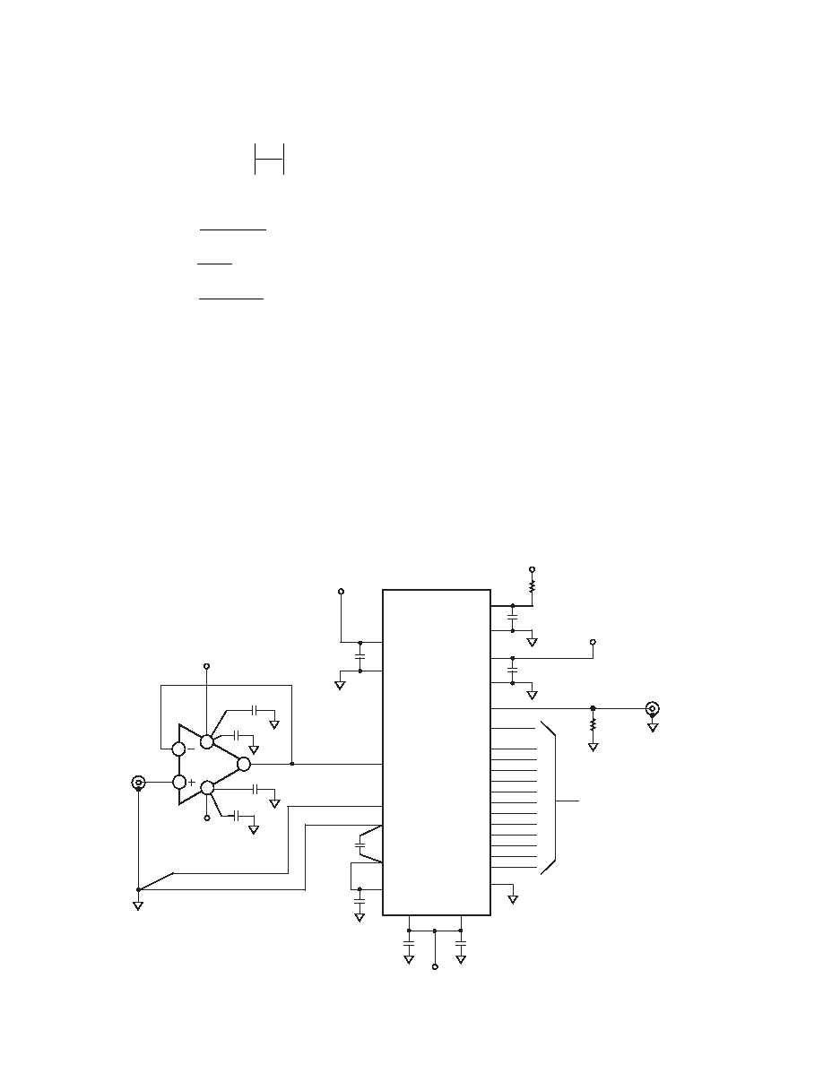
A/D Converter Driver
As A/D converters move toward higher speeds with higher reso-
lutions, there becomes a need for high performance drivers that
will not degrade the analog signal to the converter. It is desir-
able from a system’s standpoint that the A/D be the element in
the signal chain that ultimately limits overall distortion. This
places new demands on the amplifiers used to drive fast, high
resolution A/Ds.
With high bandwidth, low distortion, and fast settling time,
the AD8047 and AD8048 make high performance A/D drivers
for advanced converters. Figure 12 is an example of an AD8047
used as an input driver for an AD872A, a 12-bit, 10 MSPS
A/D converter.
MSB
BIT2
BIT3
BIT4
BIT5
BIT6
BIT7
BIT8
BIT9
BIT10
BIT11
BIT12
AVDD
AGND
VINA
REF GND
REF IN
REF OUT
AVSS
AGND
OTR
CLK
DRGND
DRVDD
DGND
DVDD
19
18
17
16
15
14
13
12
11
10
9
8
24
25
3
26
28
27
1
20
21
23
22
6
7
4
5
VINB
–5V ANALOG
AD872A
+5V ANALOG
ANALOG IN
DIGITAL OUTPUT
0.1 F
1 F
10
49.9
CLOCK INPUT
+5V ANALOG
+5V DIGITAL
2
–5V
ANALOG
10 F
0.1 F
AD8047
3
2
7
6
4
Figure 12. AD8047 Used as Driver for an AD872A, a 12-Bit, 10 MSPS A/D Converter
Layout Considerations
The specified high speed performance of the AD8047 and
AD8048 requires careful attention to board layout and compo-
nent selection. Proper RF design techniques and low-pass
parasitic component selection are mandatory.
The PCB should have a ground plane covering all unused por-
tions of the component side of the board to provide a low
impedance path. The ground plane should be removed from the
area near the input pins to reduce stray capacitance.
Chip capacitors should be used for the supply bypassing (see
Figure 12). One end should be connected to the ground plane
and the other within 1/8 inch of each power pin. An additional
large (0.47
F to 10 F) tantalum electrolytic capacitor should
be connected in parallel, though not necessarily so close, to the
supply current for fast, large signal changes at the output.
The feedback resistor should be located close to the inverting
input pin in order to keep the stray capacitance at this node to a
minimum. Capacitance variations of less than 1 pF at the inverting
input will significantly affect high speed performance.
Stripline design techniques should be used for long signal traces
(greater than about 1 inch). These should be designed with a
characteristic impedance of 50
or 75 and be properly termi-
nated at each end.
相关PDF资料 |
PDF描述 |
|---|---|
| EL5100IW-T7 | IC OP AMP HS V-FEEDBACK SOT23-6 |
| AD8664ARZ-REEL7 | IC OPAMP GP R-R CMOS 4MHZ 14SOIC |
| C1S 3.5 | FUSE 3.5A 63V 1206 SLOW C1S |
| LT6200IS6#TRMPBF | IC OPAMP R-R I/O 165MHZ SOT23-6 |
| OP262GS-REEL7 | IC OPAMP GP R-R 15MHZ DUAL 8SOIC |
相关代理商/技术参数 |
参数描述 |
|---|---|
| AD8048-EB | 制造商:Analog Devices 功能描述: |
| AD805 | 制造商:AD 制造商全称:Analog Devices 功能描述:DATA RETIMING PHASE LOCKED LOOP |
| AD8051 | 制造商:AD 制造商全称:Analog Devices 功能描述:Low Cost, High Speed, Rail-to-Rail Amplifiers |
| AD8051_06 | 制造商:AD 制造商全称:Analog Devices 功能描述:Low Cost, High Speed, Rail-to-Rail Amplifiers |
| AD8051_07 | 制造商:AD 制造商全称:Analog Devices 功能描述:Low Cost, High Speed, Rail-to-Rail Amplifiers |
发布紧急采购,3分钟左右您将得到回复。