- 您现在的位置:买卖IC网 > PDF目录5292 > AD8052ARZ-REEL7 (Analog Devices Inc)IC OPAMP VF R-R DUAL LDIST 8SOIC PDF资料下载
参数资料
| 型号: | AD8052ARZ-REEL7 |
| 厂商: | Analog Devices Inc |
| 文件页数: | 9/25页 |
| 文件大小: | 0K |
| 描述: | IC OPAMP VF R-R DUAL LDIST 8SOIC |
| 标准包装: | 750 |
| 放大器类型: | 电压反馈 |
| 电路数: | 2 |
| 输出类型: | 满摆幅 |
| 转换速率: | 170 V/µs |
| -3db带宽: | 110MHz |
| 电流 - 输入偏压: | 1.4µA |
| 电压 - 输入偏移: | 1800µV |
| 电流 - 电源: | 4.8mA |
| 电流 - 输出 / 通道: | 45mA |
| 电压 - 电源,单路/双路(±): | 3 V ~ 12 V,±1.5 V ~ 6 V |
| 工作温度: | -40°C ~ 125°C |
| 安装类型: | 表面贴装 |
| 封装/外壳: | 8-SOIC(0.154",3.90mm 宽) |
| 供应商设备封装: | 8-SO |
| 包装: | 带卷 (TR) |
AD8051/AD8052/AD8054
Rev. J | Page 16 of 24
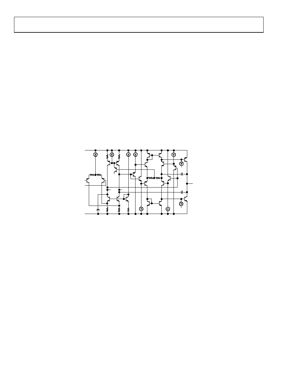
THEORY OF OPERATION
CIRCUIT DESCRIPTION
The AD8051/AD8052/AD8054 are fabricated on the Analog
Devices, Inc. proprietary eXtra-Fast Complementary Bipolar
(XFCB) process, which enables the construction of PNP and
NPN transistors with similar fTs in the 2 GHz to 4 GHz region.
The process is dielectrically isolated to eliminate the parasitic
and latch-up problems caused by junction isolation. These
features allow the construction of high frequency, low distortion
amplifiers with low supply currents. This design uses a differential
output input stage to maximize bandwidth and headroom (see
Figure 40). The smaller signal swings required on the first stage
outputs (nodes SIP, SIN) reduce the effect of nonlinear currents
due to junction capacitances and improve the distortion per-
formance. This design achieves harmonic distortion of 80 dBc
@ 1 MHz into 100 Ω with VOUT = 2 V p-p (gain = +1) on a
single 5 V supply.
The inputs of the device can handle voltages from 0.2 V below
the negative rail to within 1 V of the positive rail. Exceeding
these values do not cause phase reversal; however, the input
ESD devices begin to conduct if the input voltages exceed the
rails by greater than 0.5 V. During this overdrive condition, the
output stays at the rail.
The rail-to-rail output range of the AD8051/AD8052/AD8054
is provided by a complementary common emitter output stage.
High output drive capability is provided by injecting all output
stage predriver currents directly into the bases of the output
devices Q8 and Q36. Biasing of Q8 and Q36 is accomplished by
I8 and I5, along with a common-mode feedback loop (not
shown). This circuit topology allows the AD8051/AD8052 to
drive 45 mA of output current and allows the AD8054 to drive
30 mA of output current with the outputs within 0.5 V of the
supply rails.
I10
R39
VEE
I2
I3
Q25
Q51
R23 R27
I9
Q36
I5
VEE
C3
C9
I8
VCC
I11
I7
R3
R21
R5
Q3
SIP
SIN
C7
Q4
R15 R2
R26
Q50
Q22
Q21
Q27
Q7
Q8
Q23
Q31
Q39
Q13
Q1
Q24
Q47
Q11
Q2
Q5
Q40
VOUT
VCC
VINP
VINN
VEE
01
06
2-
04
5
Figure 40. AD8051/AD8052 Simplified Schematic
相关PDF资料 |
PDF描述 |
|---|---|
| PPPC141LGBN-RC | CONN FEMALE 14POS .100" R/A GOLD |
| LT6200IS6-5#TR | IC OP AMP 800MHZ R-R I/O SOT23-6 |
| NPPN031FGGN-RC | CONN RECEPT 2MM SINGLE R/A 3POS |
| LT6200IS6-10#TRPBF | IC OP AMP 1.6GHZ R-R I/O SOT23-6 |
| LT6200IS6-10#TR | IC OP AMP 1.6GHZ R-R I/O SOT23-6 |
相关代理商/技术参数 |
参数描述 |
|---|---|
| AD8052LV | 制造商:CADEKA 制造商全称:CADEKA 功能描述:Low Cost, +2.7V to 5.5V, 260MHz Rail-to-Rail Amplifier |
| AD8052LVIMP8X | 制造商:CADEKA 制造商全称:CADEKA 功能描述:Low Cost, +2.7V to 5.5V, 260MHz Rail-to-Rail Amplifier |
| AD8052LVISO8 | 制造商:CADEKA 制造商全称:CADEKA 功能描述:Low Cost, +2.7V to 5.5V, 260MHz Rail-to-Rail Amplifier |
| AD8052LVISO8X | 功能描述:仪表放大器 DUAL VOLTAGE FEEDBCK RAIL TO RAIL RoHS:否 制造商:Texas Instruments 通道数量: 输入补偿电压:150 V 可用增益调整: 最大输入电阻:10 kOhms 共模抑制比(最小值):88 dB 工作电源电压:2.7 V to 36 V 电源电流:200 uA 最大工作温度:+ 125 C 最小工作温度:- 40 C 封装 / 箱体:MSOP-8 封装:Bulk |
| AD8052RM | 制造商:未知厂家 制造商全称:未知厂家 功能描述:Voltage-Feedback Operational Amplifier |
发布紧急采购,3分钟左右您将得到回复。