参数资料
| 型号: | AD8062ARMZ-R7 |
| 厂商: | Analog Devices Inc |
| 文件页数: | 8/20页 |
| 文件大小: | 0K |
| 描述: | IC OPAMP VF R-R DUAL LP 8MSOP |
| 标准包装: | 1 |
| 放大器类型: | 电压反馈 |
| 电路数: | 2 |
| 输出类型: | 满摆幅 |
| 转换速率: | 650 V/µs |
| -3db带宽: | 320MHz |
| 电流 - 输入偏压: | 3.5µA |
| 电压 - 输入偏移: | 1000µV |
| 电流 - 电源: | 6.8mA |
| 电流 - 输出 / 通道: | 50mA |
| 电压 - 电源,单路/双路(±): | 2.7 V ~ 8 V,±1.35 V ~ 4 V |
| 工作温度: | -40°C ~ 85°C |
| 安装类型: | 表面贴装 |
| 封装/外壳: | 8-TSSOP,8-MSOP(0.118",3.00mm 宽) |
| 供应商设备封装: | 8-MSOP |
| 包装: | 标准包装 |
| 产品目录页面: | 770 (CN2011-ZH PDF) |
| 其它名称: | AD8062ARMZ-R7DKR |
AD8061/AD8062/AD8063
Data Sheet
Rev. J | Page 16 of 20
CAPACITIVE LOAD DRIVE
The AD8061/AD8062/AD8063 family is optimized for
bandwidth and speed, not for driving capacitive loads. Output
capacitance creates a pole in the amplifier’s feedback path,
leading to excessive peaking and potential oscillation. If dealing
with load capacitance is a requirement of the application, the
two strategies to consider are as follows:
Use a small resistor in series with the amplifier’s output and the
load capacitance.
Reduce the bandwidth of the amplifier’s feedback loop by
increasing the overall noise gain.
Figure 50 shows a unity-gain follower using the series resistor
strategy. The resistor isolates the output from the capacitance
and, more importantly, creates a zero in the feedback path that
compensates for the pole created by the output capacitance.
AD8061
VO
RSERIES
CLOAD
VIN
01065-
050
Figure 50. Series Resistor Isolating Capacitive Load
Voltage feedback amplifiers like those in the AD8061/AD8062/
AD8063 family are able to drive more capacitive load without
excessive peaking when used in higher gain configurations
because the increased noise gain reduces the bandwidth of the
overall feedback loop. Figure 51 plots the capacitance that
produces 30% overshoot vs. noise gain for a typical amplifier.
CLOSED-LOOP GAIN
10k
1k
10
1
5
2
CA
P
A
C
ITIV
E
LOA
D
(
pF)
100
3
4
RS = 0
RS = 4.7
01065-
051
Figure 51. Capacitive Load vs. Closed-Loop Gain
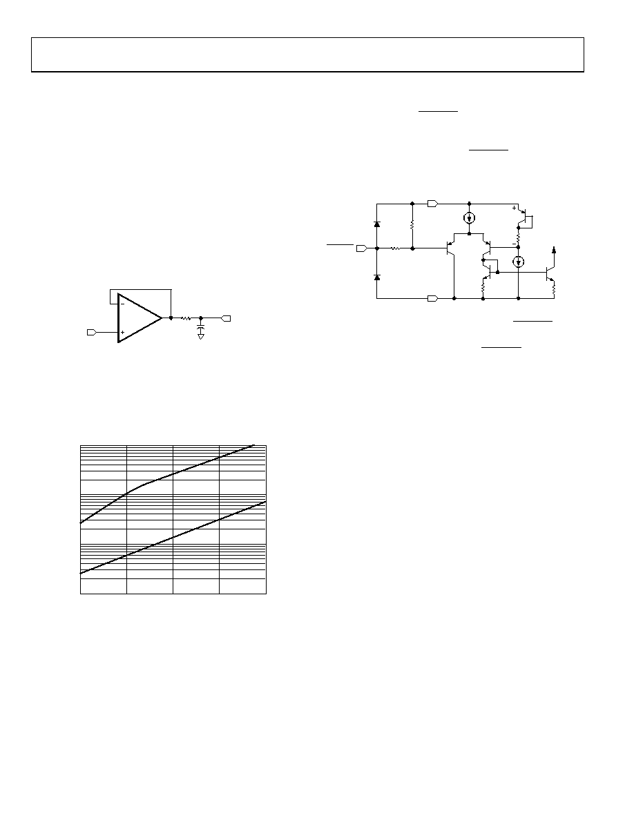
DISABLE OPERATION
The internal circuit for the AD8063 disable function is shown
in Figure 52. When the DISABLE node is pulled below 2 V
from the positive supply, the supply current decreases from
typically 6.5 mA to under 400 A, and the AD8063 output
enters a high impedance state. If the DISABLE node is not
connected and allowed to float, the AD8063 stays biased at
full power.
VCC
DISABLE
TO AMPLIFIER
BIAS
VEE
2V
01065-
052
Figure 52. Disable Circuit of the AD8063
Figure 34 shows the AD8063 supply current vs. DISABLE
voltage. Figure 35 plots the output seen when the AD8063 input
is driven with a 10 MHz sine wave, and DISABLE is toggled
from 0 V to 5 V, illustrating the part’s turn-on and turn-off
time. Figure 33 shows the input/output isolation response with
the AD8063 shut off.
BOARD LAYOUT CONSIDERATIONS
Maintaining the high speed performance of the AD8061/AD8062/
AD8063 family requires the use of high speed board layout
techniques and low parasitic components.
The PCB should have a ground plane covering unused portions
of the component side of the board to provide a low impedance
path. Remove the ground plane near the package to reduce
parasitic capacitance.
Proper bypassing is critical. Use a ceramic 0.1 F chip capacitor
to bypass both supplies. Locate the chip capacitor within 3 mm
of each power pin. Additionally, connect in parallel a 4.7 F to
10 F tantalum electrolytic capacitor to provide charge for fast,
large signal changes at the output.
Minimizing parasitic capacitance at the amplifier’s inverting
input pin is very important. Locate the feedback resistor close to
the inverting input pin. The value of the feedback resistor may
come into play—for instance, 1 k interacting with 1 pF of
parasitic capacitance creates a pole at 159 MHz. Use stripline
design techniques for signal traces longer than 25 mm. Design
them with either 50 or 75 characteristic impedance and
proper termination at each end.
相关PDF资料 |
PDF描述 |
|---|---|
| 9-146282-0-16 | CONN HDR BRKWAY .100 16POS VERT |
| 4-103741-0-16 | CONN HEADR BRKWAY .100 16POS STR |
| LTC6101HVACS5#TRMPBF | IC AMP CURRENT SENSE TSOT23-5 |
| 68021-110HLF | CONN HEADER 10POS .100 R/A 30AU |
| ADA4841-1YRZ-R7 | IC OPAMP VF R-R LP LN 60MA 8SOIC |
相关代理商/技术参数 |
参数描述 |
|---|---|
| AD8062ARMZ-RL | 功能描述:IC OPAMP VF R-R DUAL LP 8MSOP RoHS:是 类别:集成电路 (IC) >> Linear - Amplifiers - Instrumentation 系列:- 标准包装:50 系列:- 放大器类型:通用 电路数:2 输出类型:满摆幅 转换速率:1.8 V/µs 增益带宽积:6.5MHz -3db带宽:4.5MHz 电流 - 输入偏压:5nA 电压 - 输入偏移:100µV 电流 - 电源:65µA 电流 - 输出 / 通道:35mA 电压 - 电源,单路/双路(±):1.8 V ~ 5.25 V,±0.9 V ~ 2.625 V 工作温度:-40°C ~ 85°C 安装类型:表面贴装 封装/外壳:10-TFSOP,10-MSOP(0.118",3.00mm 宽) 供应商设备封装:10-MSOP 包装:管件 |
| AD8062AR-REEL | 制造商:Analog Devices 功能描述:OP Amp Dual Volt Fdbk R-R O/P 8V 8-Pin SOIC N T/R 制造商:Rochester Electronics LLC 功能描述:SOIC DUAL, RAIL-TO-RAIL VLTG-FDBK AMP - Tape and Reel |
| AD8062AR-REEL7 | 制造商:Analog Devices 功能描述:OP Amp Dual Volt Fdbk R-R O/P 8V 8-Pin SOIC N T/R 制造商:Rochester Electronics LLC 功能描述:SOIC DUAL, RAIL-TO-RAIL VLTG-FDBK AMP - Tape and Reel |
| AD8062ARZ | 功能描述:IC OPAMP VF R-R DUAL LP 8SOIC RoHS:是 类别:集成电路 (IC) >> Linear - Amplifiers - Instrumentation 系列:- 产品培训模块:Differential Circuit Design Techniques for Communication Applications 标准包装:1 系列:- 放大器类型:RF/IF 差分 电路数:1 输出类型:差分 转换速率:9800 V/µs 增益带宽积:- -3db带宽:2.9GHz 电流 - 输入偏压:3µA 电压 - 输入偏移:- 电流 - 电源:40mA 电流 - 输出 / 通道:- 电压 - 电源,单路/双路(±):3 V ~ 3.6 V 工作温度:-40°C ~ 85°C 安装类型:表面贴装 封装/外壳:16-VQFN 裸露焊盘,CSP 供应商设备封装:16-LFCSP-VQ 包装:剪切带 (CT) 产品目录页面:551 (CN2011-ZH PDF) 其它名称:ADL5561ACPZ-R7CT |
| AD8062ARZ-R7 | 功能描述:IC OPAMP VF R-R DUAL LP 8SOIC RoHS:是 类别:集成电路 (IC) >> Linear - Amplifiers - Instrumentation 系列:- 标准包装:50 系列:- 放大器类型:通用 电路数:2 输出类型:满摆幅 转换速率:1.8 V/µs 增益带宽积:6.5MHz -3db带宽:4.5MHz 电流 - 输入偏压:5nA 电压 - 输入偏移:100µV 电流 - 电源:65µA 电流 - 输出 / 通道:35mA 电压 - 电源,单路/双路(±):1.8 V ~ 5.25 V,±0.9 V ~ 2.625 V 工作温度:-40°C ~ 85°C 安装类型:表面贴装 封装/外壳:10-TFSOP,10-MSOP(0.118",3.00mm 宽) 供应商设备封装:10-MSOP 包装:管件 |
发布紧急采购,3分钟左右您将得到回复。