参数资料
| 型号: | AD8123ACPZ |
| 厂商: | Analog Devices Inc |
| 文件页数: | 6/16页 |
| 文件大小: | 0K |
| 描述: | IC RCVR TRPL DIFF EQUAL 40LFCSP |
| 标准包装: | 1 |
| 类型: | 接收器 |
| 驱动器/接收器数: | 0/3 |
| 电源电压: | 4.5 V ~ 5.5 V |
| 安装类型: | 表面贴装 |
| 封装/外壳: | 40-VFQFN 裸露焊盘,CSP |
| 供应商设备封装: | 40-LFCSP-VQ(6x6) |
| 包装: | 托盘 |
AD8123
Rev. A | Page 14 of 16
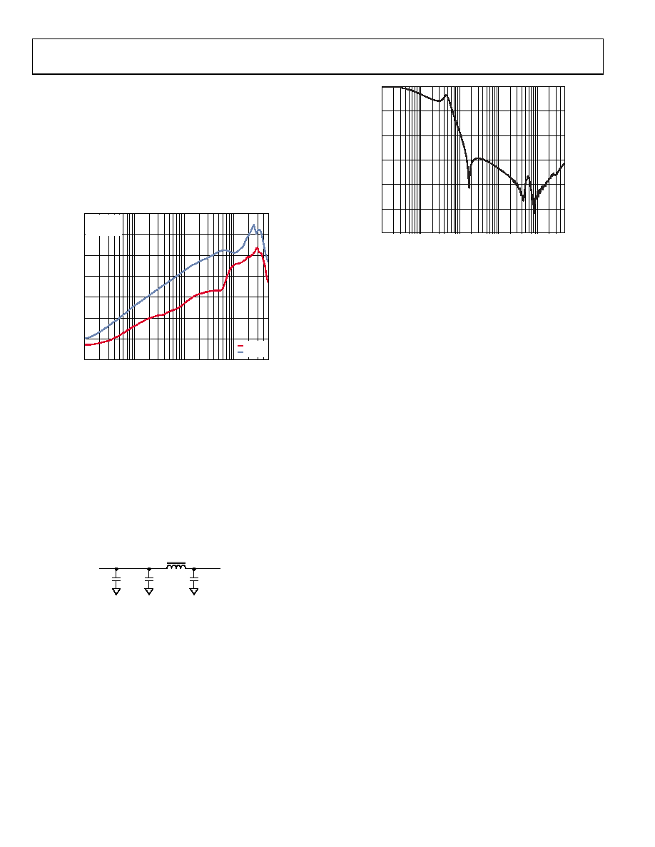
POWER SUPPLY FILTERING
External power supply filtering between the system power
supplies and the AD8123 is required in most applications to
prevent supply noise from contaminating the received signal as
well as to prevent unwanted feedback through the supplies that
could cause instability. Figure 29 shows that the AD8123 power
supply rejection decreases with increasing frequency. These
plots are for the lowest control settings and shift upward as the
peaking is increased.
–60
–50
–40
–30
–20
–10
0
10
+PSRR
–PSRR
100k
1M
10M
100M
0
681
4-
0
17
FREQUENCY (Hz)
P
S
RR
(
d
B)
VGAIN = 0V
VPEAK = 0V
VPOLE = 0V
Figure 29. AD8123 PSRR vs. Frequency
A suitable filter that uses a surface-mount ferrite bead is shown
Because the frequency response was taken using a 50 Ω network
analyzer and with only one 0.1 μF capacitor on the AD8123
side, the actual amount of rejection provided by the filter in a
real-world application will be different from that shown in
Figure 31. The general shape of the rejection curve, however,
matches Figure 31, providing substantially increased overall
PSRR from approximately 5 MHz to 500 MHz, where it is most
needed. One filter is required on each of the two supplies (not one
filter per supply pin).
FAIR-RITE
2743021447
*ALL AD8123 SUPPLY PINS ARE INDIVIDUALLY
DECOUPLED WITH A 0.1F CAPACITOR.
06
81
4-
03
1
0.1F
4700pF
SYSTEM
SUPPLY
TO AD8123*
Figure 30. Power Supply Filter
–120
–100
–80
–60
–40
–20
0
10k
100k
1M
10M
100M
068
14
-018
FREQUENCY (Hz)
O
U
TPU
T
R
E
S
P
ON
SE
(dB
)
Figure 31. Power Supply Filter Frequency Response in a 50 Ω System
LAYOUT AND POWER SUPPLY DECOUPLING
CONSIDERATIONS
Standard high speed PCB layout practices should be adhered
to when designing with the AD8123. A solid ground plane is
required and controlled impedance traces should be used when
interconnecting the high speed signals. Source termination
resistors on all of the outputs must be placed as close as possible
to the output pins.
The exposed paddle on the underside of the AD8123 must be
connected to a pad that connects to at least one PCB plane.
Several thermal vias should be used to make the connection
between the pad and the plane(s).
High quality 0.1 μF power supply decoupling capacitors should
be placed as close as possible to all of the supply pins. Small
surface-mount ceramic capacitors should be used for these, and
tantalum capacitors are recommended for bulk supply decoupling.
相关PDF资料 |
PDF描述 |
|---|---|
| AD8124ACPZ | IC HS RCVR EQUALIZER 40VFQFN |
| AD8128ACPZ-R7 | IC RECEIVER LINE EQUAL 8LFCSP |
| AD8143ACPZ-REEL7 | IC RECEIVER TRIPLE DIFF 32LFCSP |
| AD8145WYCPZ-R7 | IC RECEIVER TRIPLE DIFF 32LFCSP |
| AD8150ASTZ | IC CROSSPOINT SWIT 33X17 184LQFP |
相关代理商/技术参数 |
参数描述 |
|---|---|
| AD8123ACPZ1 | 制造商:AD 制造商全称:Analog Devices 功能描述:Triple Differential Receiver with Adjustable Line Equalization |
| AD8123ACPZR2 | 制造商:Analog Devices 功能描述:Differential Receiver Amplifier 40-Pin LFCSP EP T/R |
| AD8123ACPZ-R2 | 制造商:Analog Devices 功能描述: |
| AD8123ACPZ-R7 | 功能描述:IC RCVR TRPL DIFF EQUAL 40LFCSP RoHS:是 类别:集成电路 (IC) >> 接口 - 驱动器,接收器,收发器 系列:- 产品培训模块:RS-232 & USB Transceiver 标准包装:2,000 系列:- 类型:收发器 驱动器/接收器数:1/1 规程:RS232 电源电压:3 V ~ 5.5 V 安装类型:表面贴装 封装/外壳:16-SSOP(0.209",5.30mm 宽) 供应商设备封装:16-SSOP 包装:带卷 (TR) 其它名称:296-19849-2 |
| AD8123ACPZ-R71 | 制造商:AD 制造商全称:Analog Devices 功能描述:Triple Differential Receiver with Adjustable Line Equalization |
发布紧急采购,3分钟左右您将得到回复。