- 您现在的位置:买卖IC网 > PDF目录5305 > AD8129ARZ-REEL7 (Analog Devices Inc)IC AMP DIFF LN LDIST 40MA 8SOIC PDF资料下载
参数资料
| 型号: | AD8129ARZ-REEL7 |
| 厂商: | Analog Devices Inc |
| 文件页数: | 29/41页 |
| 文件大小: | 0K |
| 描述: | IC AMP DIFF LN LDIST 40MA 8SOIC |
| 标准包装: | 1,000 |
| 放大器类型: | 差分 |
| 电路数: | 1 |
| 转换速率: | 1070 V/µs |
| -3db带宽: | 200MHz |
| 电流 - 输入偏压: | 500nA |
| 电压 - 输入偏移: | 200µV |
| 电流 - 电源: | 13mA |
| 电流 - 输出 / 通道: | 40mA |
| 电压 - 电源,单路/双路(±): | 4.5 V ~ 25.2 V,±2.25 V ~ 12.6 V |
| 工作温度: | -40°C ~ 85°C |
| 安装类型: | 表面贴装 |
| 封装/外壳: | 8-SOIC(0.154",3.90mm 宽) |
| 供应商设备封装: | 8-SO |
| 包装: | 带卷 (TR) |
第1页第2页第3页第4页第5页第6页第7页第8页第9页第10页第11页第12页第13页第14页第15页第16页第17页第18页第19页第20页第21页第22页第23页第24页第25页第26页第27页第28页当前第29页第30页第31页第32页第33页第34页第35页第36页第37页第38页第39页第40页第41页
AD8129/AD8130
Rev. C | Page 34 of 40
RF
1k
Ω
0.1
μF
10
μF
–V
VOUT
+V
0.1
μF
10
μF
VIN
R1
100
Ω
RG
499
Ω
–VS
PD
+VS
+
C1
200pF
AD8130
100
Ω
6
2
5
4
8
1
37
02464-135
Figure 134. An Equalizer Circuit for Composite Video Transmissions
over 300 Meters of Category-5 Cable
20
10
–10
–20
–30
–40
–50
–60
–70
–80
FREQUENCY (Hz)
I/O
R
ESPON
S
E
0
10k
100k
1M
10M
100M
02464-136
Figure 135. Transmission Response of 300 Meters of Category-5 Cable
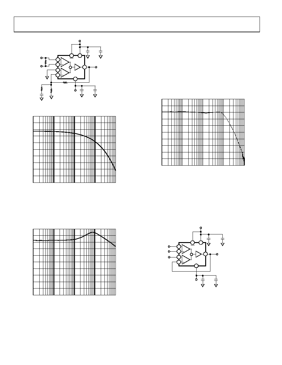
The feedback network is between Pin 6 and Pin 5 and from
Pin 5 to ground. C1 and RF create a corner frequency of about
800 kHz. The gain increases to provide about 15 dB of boost
at 8 MHz. The response of this circuit is shown in Figure 136.
20
10
–10
–20
–30
–40
–50
–60
–70
–80
FREQUENCY (Hz)
I/O
R
ESPON
S
E
0
10k
100k
1M
10M
100M
02464-137
Figure 136. Frequency Response of Equalizer Circuit
It is difficult to calculate the exact component values via strictly
mathematical means, because the equations for the cable
attenuation are approximate and have functions that are not
simply related to the responses of RC networks. The method
used in this design was to approximate the required response
via graphical means from the frequency response and then
select components that would approximate this response. The
circuit was then built, measured, and finally adjusted to obtain
an acceptable response—in this case, flat to 9 MHz to within
approximately 1 dB (see Figure 137).
20
10
–10
–20
–30
–40
–50
–60
–70
–80
FREQUENCY (Hz)
I/O
R
ESPON
S
E
0
10k
100k
1M
10M
100M
02464-138
Figure 137. Combined Response of Cable Plus Equalizer
OUTPUT OFFSET/LEVEL TRANSLATOR
The circuit in Figure 133 has the reference input (Pin 4) tied to
ground, which produces a ground-referenced output signal. If it
is desired to offset the output voltage from ground, the REF
the output with unity gain.
0.1
μF
–V
VOUT = VIN +VOFFSET
+V
0.1
μF
10
μF
VIN
VOFFSET
–VS
PD
+VS
+
AD8130
10
μF
6
2
5
4
8
1
37
02464-139
Figure 138. The Voltage Applied to Pin 4 to the Unity-Gain Output Voltage
Produced by VIN
If the circuit has a gain higher than unity, the gain must be
factored in. If RG is connected to ground, the voltage applied to
REF is multiplied by the gain of the circuit and appears at the
output—just like a noninverting conventional op amp. This
situation is not always desirable; the user may want VOFFSET to
appear at the output with unity gain.
相关PDF资料 |
PDF描述 |
|---|---|
| EL8170ISZ-T7 | IC AMP INST SGL R-R MCRPWR 8SOIC |
| 0001.2705.11 | FUSE 1.25A 250V 5X20 T-LAG SMD |
| AD8129ARMZ-REEL7 | IC AMP DIFF LN LDIST 40MA 8MSOP |
| 0001.2707.11 | FUSE 2A 250V 5X20 T-LAG SMD |
| 0001.2706.11 | FUSE 1.6A 250V 5X20 T-LAG SMD |
相关代理商/技术参数 |
参数描述 |
|---|---|
| AD8129-EVAL | 制造商:Analog Devices 功能描述:AD8129 EVALUATION BOARD |
| AD812AN | 制造商:Analog Devices 功能描述:OP Amp Dual Current Fdbk 制造商:Rochester Electronics LLC 功能描述:DUAL LO PWR I-FDBK OP AMP - Bulk 制造商:Analog Devices 功能描述:IC OP-AMP LOW POWER |
| AD812ANZ | 功能描述:IC OPAMP DUAL CURR-FDBK 8-DIP RoHS:是 类别:集成电路 (IC) >> 线性 - 放大器 - 视频放大器和频缓冲器 系列:- 产品培训模块:Lead (SnPb) Finish for COTS Obsolescence Mitigation Program 标准包装:50 系列:- 应用:TFT-LCD 面板:VCOM 驱动器 输出类型:满摆幅 电路数:1 -3db带宽:35MHz 转换速率:40 V/µs 电流 - 电源:3.7mA 电流 - 输出 / 通道:1.3A 电压 - 电源,单路/双路(±):9 V ~ 20 V,±4.5 V ~ 10 V 安装类型:表面贴装 封装/外壳:8-TSSOP,8-MSOP(0.118",3.00mm 宽)裸露焊盘 供应商设备封装:8-uMax-EP 包装:管件 |
| AD812AR | 功能描述:IC OPAMP DUAL CURR-FDBK 8-SOIC RoHS:否 类别:集成电路 (IC) >> 线性 - 放大器 - 视频放大器和频缓冲器 系列:- 标准包装:1,000 系列:- 应用:驱动器 输出类型:差分 电路数:3 -3db带宽:350MHz 转换速率:1000 V/µs 电流 - 电源:14.5mA 电流 - 输出 / 通道:60mA 电压 - 电源,单路/双路(±):5 V ~ 12 V,±2.5 V ~ 6 V 安装类型:表面贴装 封装/外壳:20-VFQFN 裸露焊盘 供应商设备封装:20-QFN 裸露焊盘(4x4) 包装:带卷 (TR) |
| AD812AR-8 | 制造商:Analog Devices 功能描述: |
发布紧急采购,3分钟左右您将得到回复。