参数资料
| 型号: | AD812AR |
| 厂商: | Analog Devices Inc |
| 文件页数: | 12/16页 |
| 文件大小: | 0K |
| 描述: | IC OPAMP DUAL CURR-FDBK 8-SOIC |
| 标准包装: | 98 |
| 应用: | 电流反馈 |
| 电路数: | 2 |
| -3db带宽: | 145MHz |
| 转换速率: | 1600 V/µs |
| 电流 - 电源: | 4.5mA |
| 电流 - 输出 / 通道: | 50mA |
| 电压 - 电源,单路/双路(±): | 2.4 V ~ 36 V,±1.2 V ~ 18 V |
| 安装类型: | 表面贴装 |
| 封装/外壳: | 8-SOIC(0.154",3.90mm 宽) |
| 供应商设备封装: | 8-SOIC |
| 包装: | 管件 |
AD812
–5–
REV. B
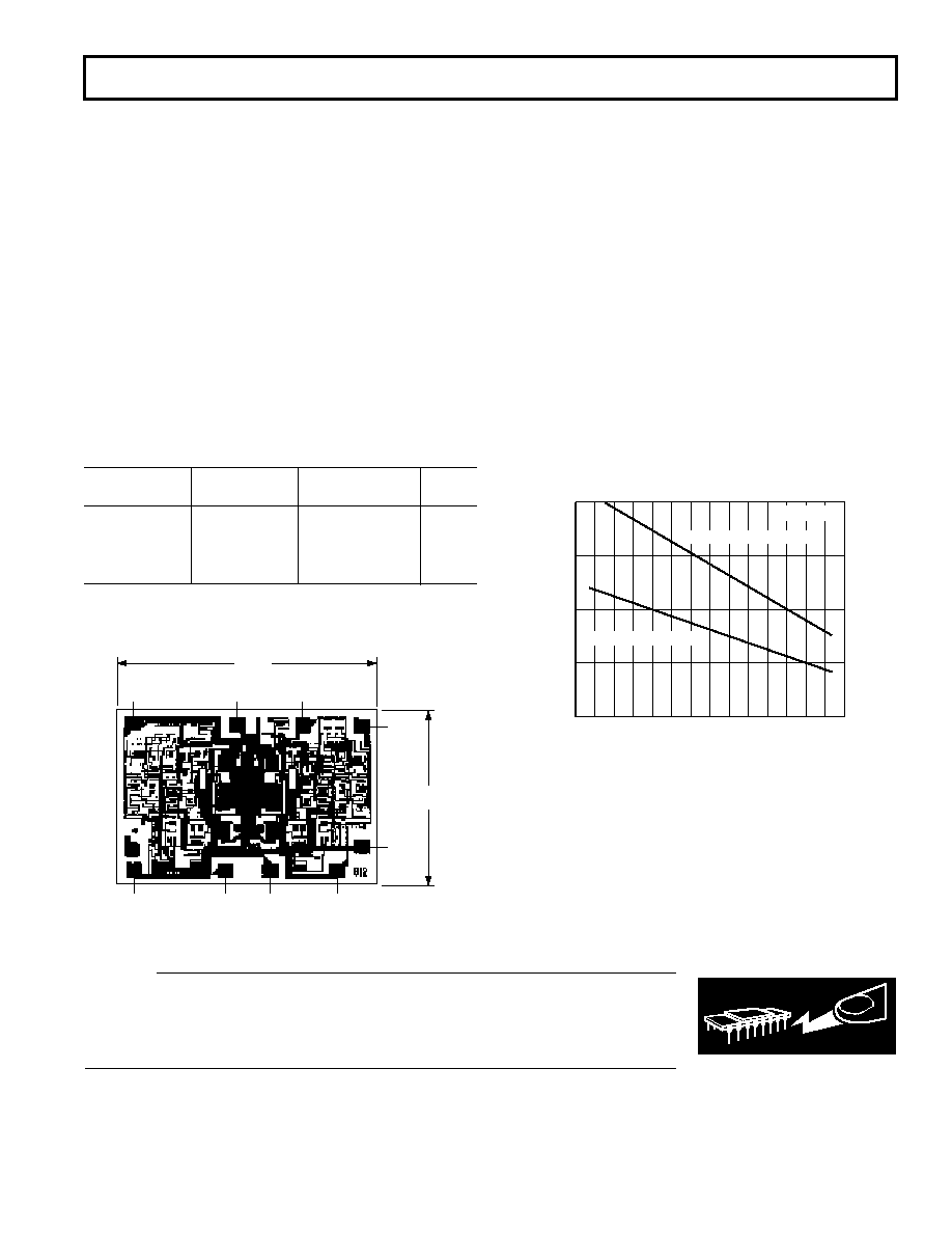
MAXIMUM POWER DISSIPATION
The maximum power that can be safely dissipated by the
AD812 is limited by the associated rise in junction temperature.
The maximum safe junction temperature for the plastic encap-
sulated parts is determined by the glass transition temperature
of the plastic, about 150
°C. Exceeding this limit temporarily
may cause a shift in parametric performance due to a change in
the stresses exerted on the die by the package. Exceeding a
junction temperature of 175
°C for an extended period can result
in device failure.
While the AD812 is internally short circuit protected, this may
not be sufficient to guarantee that the maximum junction tem-
perature (150 degrees) is not exceeded under all conditions. To
ensure proper operation, it is important to observe the derating
curves.
It must also be noted that in high (noninverting) gain configura-
tions (with low values of gain resistor), a high level of input
overdrive can result in a large input error current, which may
result in a significant power dissipation in the input stage. This
power must be included when computing the junction tempera-
ture rise due to total internal power.
MAXIMUM
POWER
DISSIPATION
–
Watts
AMBIENT TEMPERATURE – C
2.0
1.5
0
–50
90
–40 –30 –20 –10
0
10
20 30
50
60
70
80
40
1.0
0.5
8-LEAD SOIC PACKAGE
8-LEAD MINI-DIP PACKAGE
TJ = +150 C
Figure 3. Plot of Maximum Power Dissipation vs.
Temperature
ABSOLUTE MAXIMUM RATINGS
1
Supply Voltage . . . . . . . . . . . . . . . . . . . . . . . . . . . . . . . . .
±18 V
Internal Power Dissipation
2
Plastic (N) . . . . . . . . . . . . . . . . . . . . . . . . . . . . . . . 1.3 Watts
Small Outline (R) . . . . . . . . . . . . . . . . . . . . . . . . . . 0.9 Watts
Input Voltage (Common Mode) . . . . . . . . . . . . . . . . . . . .
±V
S
Differential Input Voltage . . . . . . . . . . . . . . . . . . . . . . .
±1.2 V
Output Short Circuit Duration
. . . . . . . . . . . . . . . . . . . . . . Observe Power Derating Curves
Storage Temperature Range N, R . . . . . . . . . –65
°C to +125°C
Operating Temperature Range . . . . . . . . . . . . –40
°C to +85°C
Lead Temperature Range (Soldering, 10 sec) . . . . . . . +300
°C
NOTES
1Stresses above those listed under Absolute Maximum Ratings may cause perma-
nent damage to the device. This is a stress rating only; functional operation of the
device at these or any other conditions above those indicated in the operational
section of this specification is not implied. Exposure to absolute maximum rating
conditions for extended periods may affect device reliability.
2Specification is for device in free air: 8-lead plastic package:
θ
JA = 90°C/Watt;
8-lead SOIC package:
θ
JA = 150°C/Watt.
ORDERING GUIDE
Temperature
Package
Model
Range
Description
Option
AD812AN
–40
°C to +85°C
8-Lead Plastic DIP
N-8
AD812AR
–40
°C to +85°C
8-Lead Plastic SOIC SO-8
AD812AR-REEL
13" Reel
AD812AR-REEL7
7" Reel
METALIZATION PHOTO
Dimensions shown in inches and (mm).
V+
8
OUT2
7
–IN2
6
2
–IN1
3
+IN1
4
V–
1
OUT1
5 +IN2
4 V–
0.0783
(1.99)
0.0539
(1.37)
CAUTION
ESD (electrostatic discharge) sensitive device. Electrostatic charges as high as 4000 V readily
accumulate on the human body and test equipment and can discharge without detection.
Although the AD812 features proprietary ESD protection circuitry, permanent damage may
occur on devices subjected to high energy electrostatic discharges. Therefore, proper ESD
precautions are recommended to avoid performance degradation or loss of functionality.
WARNING!
ESD SENSITIVE DEVICE
相关PDF资料 |
PDF描述 |
|---|---|
| AD8138ARM | IC AMP DIFF LDIST LP 95MA 8MSOP |
| AD813AR-14 | IC TRPL VIDEO AMP SNGL LP 14SOIC |
| AD8141ACPZ-RL | IC VIDEO AMP TRPL DIFF 24LFCSP |
| AD8147ACPZ-R2 | IC DRIVER TRPL DIFF VID 24-LFCSP |
| AD817AR | IC OPAMP HS LP 8-SOIC |
相关代理商/技术参数 |
参数描述 |
|---|---|
| AD812AR-8 | 制造商:Analog Devices 功能描述: |
| AD812AR-EBZ | 功能描述:BOARD EVAL FOR AD812AR RoHS:是 类别:编程器,开发系统 >> 评估演示板和套件 系列:* 标准包装:1 系列:- 主要目的:电信,线路接口单元(LIU) 嵌入式:- 已用 IC / 零件:IDT82V2081 主要属性:T1/J1/E1 LIU 次要属性:- 已供物品:板,电源,线缆,CD 其它名称:82EBV2081 |
| AD812AR-REEL | 功能描述:IC OPAMP DUAL CURR-FDBK 8-SOIC RoHS:否 类别:集成电路 (IC) >> 线性 - 放大器 - 视频放大器和频缓冲器 系列:- 标准包装:1,000 系列:- 应用:驱动器 输出类型:差分 电路数:3 -3db带宽:350MHz 转换速率:1000 V/µs 电流 - 电源:14.5mA 电流 - 输出 / 通道:60mA 电压 - 电源,单路/双路(±):5 V ~ 12 V,±2.5 V ~ 6 V 安装类型:表面贴装 封装/外壳:20-VFQFN 裸露焊盘 供应商设备封装:20-QFN 裸露焊盘(4x4) 包装:带卷 (TR) |
| AD812AR-REEL7 | 功能描述:IC OPAMP DUAL CURR-FDBK 8-SOIC RoHS:否 类别:集成电路 (IC) >> 线性 - 放大器 - 视频放大器和频缓冲器 系列:- 标准包装:1,000 系列:- 应用:驱动器 输出类型:差分 电路数:3 -3db带宽:350MHz 转换速率:1000 V/µs 电流 - 电源:14.5mA 电流 - 输出 / 通道:60mA 电压 - 电源,单路/双路(±):5 V ~ 12 V,±2.5 V ~ 6 V 安装类型:表面贴装 封装/外壳:20-VFQFN 裸露焊盘 供应商设备封装:20-QFN 裸露焊盘(4x4) 包装:带卷 (TR) |
| AD812ARZ | 功能描述:IC OPAMP DUAL CURR-FDBK 8-SOIC RoHS:是 类别:集成电路 (IC) >> 线性 - 放大器 - 视频放大器和频缓冲器 系列:- 产品培训模块:Lead (SnPb) Finish for COTS Obsolescence Mitigation Program 标准包装:50 系列:- 应用:TFT-LCD 面板:VCOM 驱动器 输出类型:满摆幅 电路数:1 -3db带宽:35MHz 转换速率:40 V/µs 电流 - 电源:3.7mA 电流 - 输出 / 通道:1.3A 电压 - 电源,单路/双路(±):9 V ~ 20 V,±4.5 V ~ 10 V 安装类型:表面贴装 封装/外壳:8-TSSOP,8-MSOP(0.118",3.00mm 宽)裸露焊盘 供应商设备封装:8-uMax-EP 包装:管件 |
发布紧急采购,3分钟左右您将得到回复。