- 您现在的位置:买卖IC网 > PDF目录8538 > AD812ARZ-REEL7 (Analog Devices Inc)IC OPAMP DUAL CURR-FDBK 8-SOIC PDF资料下载
参数资料
| 型号: | AD812ARZ-REEL7 |
| 厂商: | Analog Devices Inc |
| 文件页数: | 6/16页 |
| 文件大小: | 0K |
| 描述: | IC OPAMP DUAL CURR-FDBK 8-SOIC |
| 标准包装: | 750 |
| 应用: | 电流反馈 |
| 电路数: | 2 |
| -3db带宽: | 145MHz |
| 转换速率: | 1600 V/µs |
| 电流 - 电源: | 4.5mA |
| 电流 - 输出 / 通道: | 50mA |
| 电压 - 电源,单路/双路(±): | 2.4 V ~ 36 V,±1.2 V ~ 18 V |
| 安装类型: | 表面贴装 |
| 封装/外壳: | 8-SOIC(0.154",3.90mm 宽) |
| 供应商设备封装: | 8-SOIC |
| 包装: | 带卷 (TR) |
AD812
REV. B
–14–
1
10
1000
100
FREQUENCY – MHz
6
9
3
0
–3
CLOSED-LOOP
GAIN
–
dB
12
–6
–9
VS = 15V
G = +2
RF = 750
RL = 1k
CL = 510pF, RS = 15
CL = 150pF, RS = 30
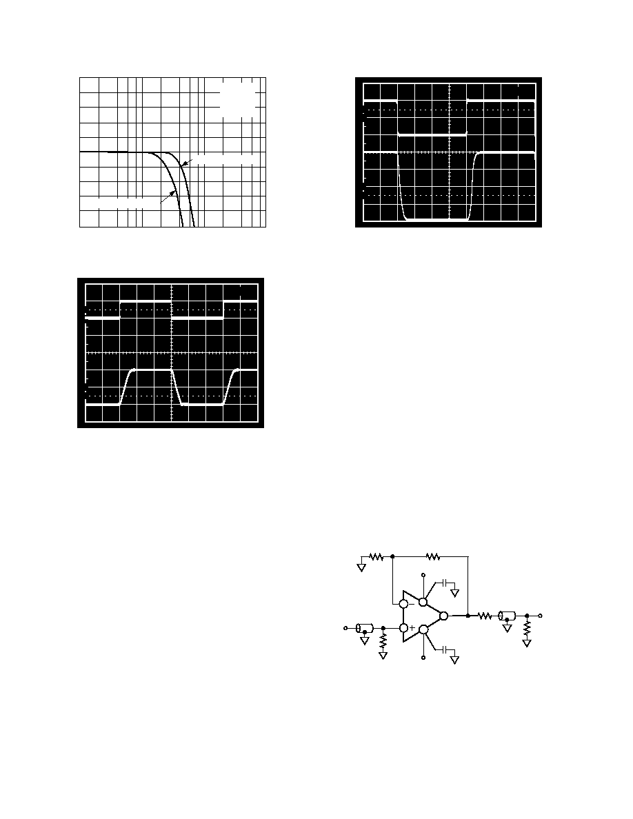
Figure 43. Response to Large Load Capacitor, VS = ±15 V
10
100
0%
100ns
5V
VIN
VOUT
90
Figure 44. Pulse Response of Circuit of Figure 41 with
CL = 510 pF, RL = 1 k
, R
F = RG = 715
, R
S = 15
Overload Recovery
There are three important overload conditions to consider.
They are due to input common mode voltage overdrive, input
current overdrive, and output voltage overdrive. When the
amplifier is configured for low closed-loop gains, and its input
common-mode voltage range is exceeded, the recovery time will
be very fast, typically under 10 ns. When configured for a higher
gain, and overloaded at the output, the recovery time will also
be short. For example, in a gain of +10, with 6 dB of input
overdrive, the recovery time of the AD812 is about 10 ns.
10
90
100
0%
2V
1V
50ns
VIN
VOUT
Figure 45. 6 dB Overload Recovery; G = 10, RL = 500 ,
VS = ±5 V
In the case of high gains with very high levels of input overdrive,
a longer recovery time may occur. For example, if the input
common-mode voltage range is exceeded in a gain of +10, the
recovery time will be on the order of 100 ns. This is primarily
due to current overloading of the input stage.
As noted in the warning under “Maximum Power Dissipation,”
a high level of input overdrive in a high noninverting gain circuit
can result in a large current flow in the input stage. For differ-
ential input voltages of less than about 1.25 V, this will be inter-
nally limited to less than 20 mA (decreasing with supply voltage).
For input overdrives which result in higher differential input
voltages, power dissipation in the input stage must be consid-
ered. It is recommended that external diode clamps be used in
cases where the differential input voltage is expected to exceed
1.25 V.
High Performance Video Line Driver
At a gain of +2, the AD812 makes an excellent driver for a back-
terminated 75
video line. Low differential gain and phase
errors and wide 0.1 dB bandwidth can be realized over a wide
range of power supply voltage. Outstanding gain and group
delay matching are also attainable over the full operating supply
voltage range.
AD812
8
4
RG
RF
VIN
75
VOUT
75
+VS
0.1 F
–VS
75
CABLE
75
CABLE
75
Figure 46. Gain of +2 Video Line Driver (RF = RG from
Table I)
相关PDF资料 |
PDF描述 |
|---|---|
| MAX5512EUA+T | IC DAC 8BIT DUAL VOUT 8-UMAX |
| VI-B0P-MX-S | CONVERTER MOD DC/DC 13.8V 75W |
| MAX5520ETC+ | IC DAC 10BIT SGL ULP 12-TQFN |
| 2-1877845-0 | PLUG 5POS 0 DEG GRY/RED 4.0-5.2 |
| VI-B0L-MX-S | CONVERTER MOD DC/DC 28V 75W |
相关代理商/技术参数 |
参数描述 |
|---|---|
| AD813 | 制造商:AD 制造商全称:Analog Devices 功能描述:Single Supply, Low Power Triple Video Amplifier |
| AD8130 | 制造商:AD 制造商全称:Analog Devices 功能描述:Low Cost 270 MHz Differential Receiver Amplifiers |
| AD8130AR | 功能描述:IC AMP DIFF LN LDIST 40MA 8SOIC RoHS:否 类别:集成电路 (IC) >> Linear - Amplifiers - Instrumentation 系列:- 标准包装:1 系列:- 放大器类型:通用 电路数:4 输出类型:满摆幅 转换速率:0.028 V/µs 增益带宽积:105kHz -3db带宽:- 电流 - 输入偏压:3nA 电压 - 输入偏移:100µV 电流 - 电源:3.3µA 电流 - 输出 / 通道:12mA 电压 - 电源,单路/双路(±):2.7 V ~ 12 V,±1.35 V ~ 6 V 工作温度:-40°C ~ 85°C 安装类型:表面贴装 封装/外壳:14-TSSOP(0.173",4.40mm 宽) 供应商设备封装:14-TSSOP 包装:剪切带 (CT) 其它名称:OP481GRUZ-REELCT |
| AD8130AR | 制造商:Analog Devices 功能描述:SEMICONDUCTOR ((NW)) |
| AD8130AR-EB | 制造商:Analog Devices 功能描述:LEADED EVALUATION BOARD - Boxed Product (Development Kits) |
发布紧急采购,3分钟左右您将得到回复。