参数资料
| 型号: | AD8132AR |
| 厂商: | Analog Devices Inc |
| 文件页数: | 18/33页 |
| 文件大小: | 0K |
| 描述: | IC AMP DIFF LDIST LP 70MA 8SOIC |
| 标准包装: | 98 |
| 放大器类型: | 差分 |
| 电路数: | 1 |
| 输出类型: | 差分 |
| 转换速率: | 1200 V/µs |
| -3db带宽: | 360MHz |
| 电流 - 输入偏压: | 3µA |
| 电压 - 输入偏移: | 1000µV |
| 电流 - 电源: | 12mA |
| 电流 - 输出 / 通道: | 70mA |
| 电压 - 电源,单路/双路(±): | 2.7 V ~ 11 V,±1.35 V ~ 5.5 V |
| 工作温度: | -40°C ~ 125°C |
| 安装类型: | 表面贴装 |
| 封装/外壳: | 8-SOIC(0.154",3.90mm 宽) |
| 供应商设备封装: | 8-SO |
| 包装: | 管件 |
第1页第2页第3页第4页第5页第6页第7页第8页第9页第10页第11页第12页第13页第14页第15页第16页第17页当前第18页第19页第20页第21页第22页第23页第24页第25页第26页第27页第28页第29页第30页第31页第32页第33页
AD8132
Rev. I | Page 24 of 32
When using the AD8132 in gain configurations where β1 ≠ β2,
differential output noise appears due to input-referred voltage
noise in the VOCM circuitry according to the following formula:
In cases where more accurate control of the output common-mode
level is required, it is a best practice that an external source or
resistor divider (with RSOURCE < 10 kΩ) be used. The output
common-mode offset values in the Specifications section assume
the VOCM input is driven by a low impedance voltage source.
+
=
β2
β1
β2
β1
V
NOCM
OND
2
DRIVING A CAPACITIVE LOAD
where:
VOND is the output differential noise.
VNOCM is the input-referred voltage noise on VOCM.
A purely capacitive load can react with the pin and bond wire
inductance of the AD8132, resulting in high frequency ringing
in the pulse response. One way to minimize this effect is to place a
small capacitor across each of the feedback resistors. The added
capacitance must be small to avoid destabilizing the amplifier. An
alternative technique is to place a small resistor in series with
the amplifier outputs, as shown in Figure 60.
CALCULATING INPUT IMPEDANCE OF THE
APPLICATION CIRCUIT
The effective input impedance of a circuit, such as that in Figure 64,
at +DIN and DIN, depends on whether the amplifier is being
driven by a single-ended or differential signal source. For balanced
differential input signals, the input impedance (RIN, dm) between
the inputs (+DIN and DIN) is simply
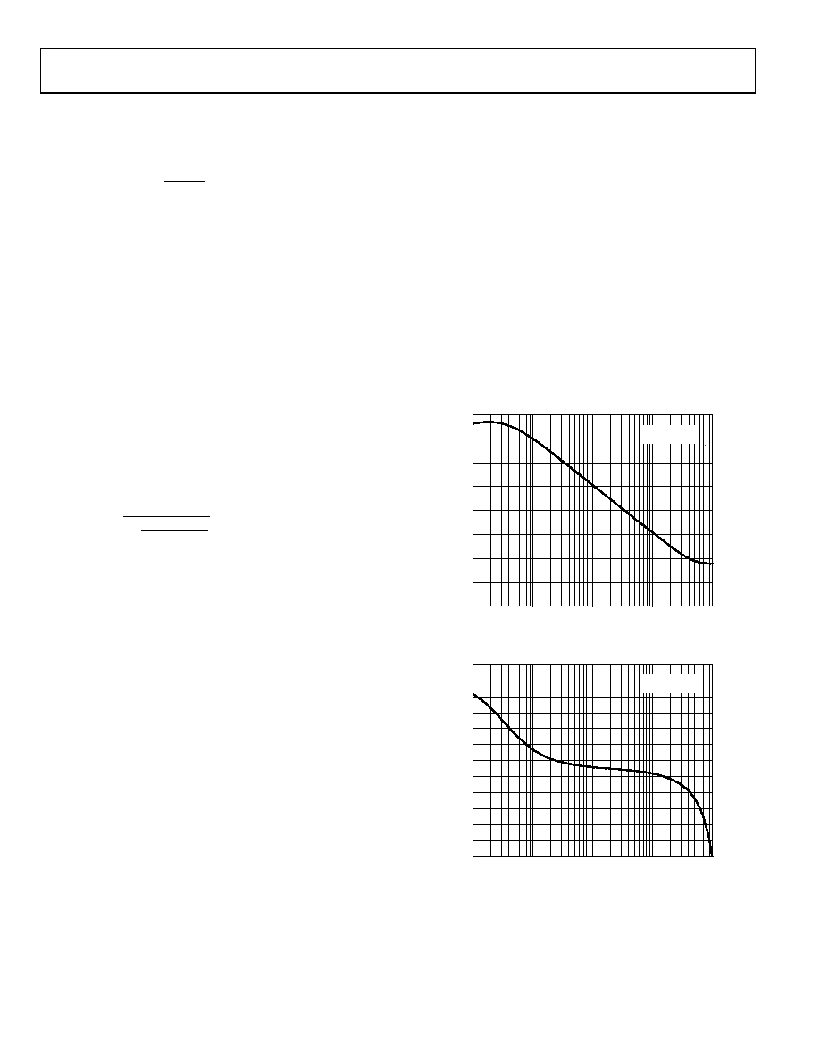
OPEN-LOOP GAIN AND PHASE
Open-loop gain and phase plots are shown in Figure 65 and
RIN, dm = 2 × RG
–20
–10
0
10
20
30
40
50
60
0.1
1
10
100
1000
FREQUENCY (MHz)
O
P
E
N
-L
OO
P
GA
IN
(d
B
)
RL, dm = 2k
01
035
-08
3
In the case of a single-ended input signal (for example, if DIN
is grounded and the input signal is applied to +DIN), the input
impedance becomes
()
+
×
=
F
G
F
G
dm
IN,
R
2
1
The circuit input impedance is effectively higher than it would
be for a conventional op amp connected as an inverter because
a fraction of the differential output voltage appears at the inputs
as a common-mode signal, partially bootstrapping the voltage
across the input resistor, RG.
Figure 65. Open-Loop Gain vs. Frequency
INPUT COMMON-MODE VOLTAGE RANGE IN
SINGLE-SUPPLY APPLICATIONS
–200
–180
–160
–140
–120
–100
–80
–60
–40
–20
0
20
40
0.1
1
10
100
1000
FREQUENCY (MHz)
O
P
E
N
-L
O
P
HAS
E
(
D
eg
rees)
RL, dm = 2k
01
03
5-
08
4
The AD8132 is optimized for level-shifting, ground-referenced
input signals. For a single-ended input, this implies that the voltage
voltage (at V) of the amplifier is also set to 0 V.
SETTING THE OUTPUT COMMON-MODE VOLTAGE
The VOCM pin of the AD8132 is internally biased at a voltage
approximately equal to the midsupply point (average value of the
voltage on V+ and V). Relying on this internal bias results in an
output common-mode voltage that is within approximately
100 mV of the expected value.
Figure 66. Open-Loop Phase vs. Frequency
相关PDF资料 |
PDF描述 |
|---|---|
| 0234010.MXP | FUSE NORM 250VAC 10A 5X20 |
| 1.5KE16AHE3/73 | TVS UNIDIRECT 1.5KW 16V 5% 1.5KE |
| 1.5KE160AHE3/73 | TVS UNIDIR 1.5KW 160V 5% 1.5KE |
| 1.5KE15AHE3/73 | TVS UNIDIR 1.5KW 15V 5% 1.5KE |
| ISL28130CEZ-T7A | IC OPAMP GP RRIO 400KHZ SC70-5 |
相关代理商/技术参数 |
参数描述 |
|---|---|
| AD8132AR | 制造商:Analog Devices 功能描述:SEMICONDUCTORS ((NW)) |
| AD8132AR-EBZ | 功能描述:BOARD EVAL FOR AD8132AR RoHS:是 类别:编程器,开发系统 >> 评估板 - 运算放大器 系列:- 产品培训模块:Lead (SnPb) Finish for COTS Obsolescence Mitigation Program 标准包装:1 系列:- |
| AD8132ARM | 功能描述:IC AMP DIFF LDIST LP 70MA 8MSOP RoHS:否 类别:集成电路 (IC) >> Linear - Amplifiers - Instrumentation 系列:- 标准包装:1 系列:- 放大器类型:通用 电路数:4 输出类型:满摆幅 转换速率:0.028 V/µs 增益带宽积:105kHz -3db带宽:- 电流 - 输入偏压:3nA 电压 - 输入偏移:100µV 电流 - 电源:3.3µA 电流 - 输出 / 通道:12mA 电压 - 电源,单路/双路(±):2.7 V ~ 12 V,±1.35 V ~ 6 V 工作温度:-40°C ~ 85°C 安装类型:表面贴装 封装/外壳:14-TSSOP(0.173",4.40mm 宽) 供应商设备封装:14-TSSOP 包装:剪切带 (CT) 其它名称:OP481GRUZ-REELCT |
| AD8132ARM-EBZ | 功能描述:BOARD EVAL FOR AD8132ARM RoHS:是 类别:编程器,开发系统 >> 评估板 - 运算放大器 系列:- 产品培训模块:Lead (SnPb) Finish for COTS Obsolescence Mitigation Program 标准包装:1 系列:- |
| AD8132ARM-REEL | 制造商:Analog Devices 功能描述:SP Amp DIFF AMP Single ±5.5V/11V 8-Pin MSOP T/R |
发布紧急采购,3分钟左右您将得到回复。