- 您现在的位置:买卖IC网 > PDF目录2136 > AD8133ACPZ-REEL (Analog Devices Inc)IC OPAMP DIFF TRPL LDIST 24LFCSP PDF资料下载
参数资料
| 型号: | AD8133ACPZ-REEL |
| 厂商: | Analog Devices Inc |
| 文件页数: | 5/16页 |
| 文件大小: | 0K |
| 描述: | IC OPAMP DIFF TRPL LDIST 24LFCSP |
| 标准包装: | 5,000 |
| 放大器类型: | 差分 |
| 电路数: | 3 |
| 输出类型: | 差分 |
| 转换速率: | 1600 V/µs |
| -3db带宽: | 450MHz |
| 电流 - 输入偏压: | 67µA |
| 电压 - 输入偏移: | 6000µV |
| 电流 - 电源: | 28mA |
| 电流 - 输出 / 通道: | 90mA |
| 电压 - 电源,单路/双路(±): | 4.5 V ~ 12 V,±2.25 V ~ 6 V |
| 工作温度: | -40°C ~ 85°C |
| 安装类型: | 表面贴装 |
| 封装/外壳: | 24-VFQFN 裸露焊盘,CSP |
| 供应商设备封装: | 24-LFCSP-VQ(4x4) |
| 包装: | 带卷 (TR) |
AD8133
Rev. 0 | Page 13 of 16
CALCULATING AN APPLICATION CIRCUIT’S INPUT
IMPEDANCE
The effective input impedance of a circuit such as that in
being driven by a single-ended or differential signal source. For
balanced differential input signals, the differential input imped-
ance, RIN, dm, between the inputs VIP and VIN is simply
kΩ
1.5
2
=
×
=
G
dm
IN,
R
In the case of a single-ended input signal (for example, if VIN is
grounded and the input signal is applied to VIP), the input
impedance becomes:
()
kΩ
125
.
1
2
1
=
+
×
=
F
G
F
G
dm
IN,
R
The circuit’s input impedance is effectively higher than it would
be for a conventional op amp connected as an inverter because
a fraction of the differential output voltage appears at the inputs
as a common-mode signal, partially bootstrapping the voltage
across the input resistor RG.
INPUT COMMON-MODE VOLTAGE RANGE IN SINGLE-
SUPPLY APPLICATIONS
The inputs of the AD8133 are designed to facilitate level-
shifting of ground referenced input signals on a single power
supply. For a single-ended input, this would imply, for example,
amplifier’s negative power supply voltage was also set to 0 V.
It is important to ensure that the common-mode voltage at the
amplifier inputs, VAP and VAN, stays within its specified range.
Since voltages VAP and VAN are driven to be essentially equal by
negative feedback, the amplifier’s input common-mode voltage
can be expressed as a single term, VACM. VACM can be calculated
as follows
3
2 ICM
OCM
ACM
V
+
=
where VICM is the common-mode voltage of the input signal, i.e.,
2
IN
IP
ICM
V
+
=
.
DRIVING A CAPACITIVE LOAD
A purely capacitive load can react with the output
impedance of the AD8133 to reduce phase margin, resulting in
high frequency ringing in the pulse response. The best way to
minimize this effect is to place a small resistor in series with
each of the amplifier’s outputs to buffer the load capacitance.
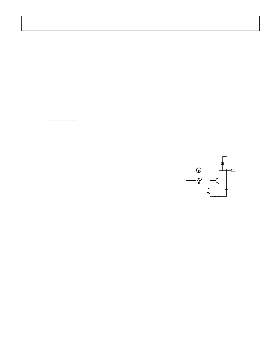
OUTPUT PULL-DOWN (OPD)
The AD8133 has an OPD pin that when pulled high signifi-
cantly reduces the power consumed while simultaneously
pulling the outputs to within less than 1 V of VS when used
with series diodes (see the Applications section). The equivalent
schematic of the output pull-down circuit is shown in Figure 35.
(The ESD diodes shown in Figure 35 are for ESD protection and
are distinct from the series diodes used with the output pull-
down feature.) See Figure 18 and Figure 21 for the output
pull-down transient and isolation performance plots. The
threshold levels for the OPD pin are referenced to the positive
power supply voltage and are presented in the Specifications
tables. When the OPD pin is pulled high, the AD8133 enters the
output low disable state.
VOUT
ESD
DIODE
ESD
DIODE
VCC
PULLDOWN
(OUTPUT IS
PULLED DOWN
WHEN SWITCH
IS CLOSED)
VS–
04769-0-004
VS+
Figure 35. Output Pull-Down Equivalent Circuit
OUTPUT COMMON-MODE CONTROL
The AD8133 allows the user to control each of the three
common-mode output levels independently through the three
VOCM input pins. The VOCM pins pass a signal to the common-
mode output level of each of their respective amplifiers with
330 MHz of small signal bandwidth and an internally fixed
gain of one. In this way, additional control and communication
signals can be embedded on the common-mode levels as the
user sees fit.
With no external circuitry, the level at the VOCM input of each
amplifier defaults to approximately midsupply. An internal
resistive divider with an impedance of approximately 100 k
sets this level. To limit common-mode noise in dc common-
mode applications, external bypass capacitors should be
connected from each of the VOCM input pins to ground.
相关PDF资料 |
PDF描述 |
|---|---|
| AD8134ACPZ-REEL | IC OPAMP DIFF TRPL LDIST 24LFCSP |
| AD8137YR | IC AMP DIFF R-R LP 20MA 8SOIC |
| AD8139ARD-REEL | IC AMP DIFF R-R LN LDIST 8SOIC |
| AD8202WYRMZ | IC AMP DIFF 50KHZ 8MSOP |
| AD8203YRZ-R7 | IC AMP DIFF 60KHZ 8SOIC |
相关代理商/技术参数 |
参数描述 |
|---|---|
| AD8133ACPZ-REEL7 | 功能描述:IC OPAMP DIFF TRPL LDIST 24LFCSP RoHS:是 类别:集成电路 (IC) >> Linear - Amplifiers - Instrumentation 系列:- 标准包装:2,500 系列:- 放大器类型:通用 电路数:2 输出类型:满摆幅 转换速率:350 V/µs 增益带宽积:180MHz -3db带宽:320MHz 电流 - 输入偏压:12.5µA 电压 - 输入偏移:800µV 电流 - 电源:15mA 电流 - 输出 / 通道:85mA 电压 - 电源,单路/双路(±):2.5 V ~ 12.6 V,±1.25 V ~ 6.3 V 工作温度:-40°C ~ 85°C 安装类型:表面贴装 封装/外壳:8-TSSOP,8-MSOP(0.118",3.00mm 宽) 供应商设备封装:8-MSOP 包装:带卷 (TR) |
| AD8134 | 制造商:AD 制造商全称:Analog Devices 功能描述:Triple Differential Driver With Sync-On-Common-Mode |
| AD8134ACP-R2 | 制造商:Analog Devices 功能描述:SP Amp DIFF Line Driver Amp Triple 制造商:Analog Devices 功能描述:SP AMP DIFF LINE DRVR AMP TRIPLE 6V/6V 24LFCSP EP - Tape and Reel |
| AD8134ACP-REEL | 制造商:AD 制造商全称:Analog Devices 功能描述:Triple Differential Driver With Sync-On-Common-Mode |
| AD8134ACP-REEL7 | 制造商:Analog Devices 功能描述:SP Amp DIFF Line Driver Amp Triple 制造商:Rochester Electronics LLC 功能描述:- Tape and Reel |
发布紧急采购,3分钟左右您将得到回复。