- 您现在的位置:买卖IC网 > PDF目录5827 > AD8139ACPZ-REEL (Analog Devices Inc)IC AMP DIFF R-R LN LDIST 8LFCSP PDF资料下载
参数资料
| 型号: | AD8139ACPZ-REEL |
| 厂商: | Analog Devices Inc |
| 文件页数: | 16/25页 |
| 文件大小: | 0K |
| 描述: | IC AMP DIFF R-R LN LDIST 8LFCSP |
| 标准包装: | 5,000 |
| 放大器类型: | 差分 |
| 电路数: | 1 |
| 输出类型: | 差分,满摆幅 |
| 转换速率: | 800 V/µs |
| -3db带宽: | 410MHz |
| 电流 - 输入偏压: | 2.25µA |
| 电压 - 输入偏移: | 150µV |
| 电流 - 电源: | 24.5mA |
| 电流 - 输出 / 通道: | 100mA |
| 电压 - 电源,单路/双路(±): | 4.5 V ~ 12 V,±2.25 V ~ 6 V |
| 工作温度: | -40°C ~ 125°C |
| 安装类型: | 表面贴装 |
| 封装/外壳: | 8-VFDFN 裸露焊盘,CSP |
| 供应商设备封装: | 8-LFCSP-VD(3x3) |
| 包装: | 带卷 (TR) |
AD8139
Rev. B | Page 22 of 24
Driving a Capacitive Load
A purely capacitive load reacts with the bondwire and pin
inductance of the AD8139, resulting in high frequency ringing
in the transient response and loss of phase margin. One way to
minimize this effect is to place a small resistor in series with
each output to buffer the load capacitance (see Figure 58 and
Figure 63). The resistor and load capacitance form a first-order,
low-pass filter; therefore, the resistor value should be as small as
possible. In some cases, the ADCs require small series resistors
to be added on their inputs.
–13
–12
–11
–10
–9
–8
–7
–6
–5
–4
–3
–2
–1
0
1
2
3
4
10M
100M
1G
5
FREQUENCY (Hz)
C
L
OS
E
D
LOO
P
GA
IN
(
d
B
)
RS = 30.1
CL = 15pF
RS = 60.4
CL = 15pF
RS = 60.4
CL = 5pF
RS = 0
CL, dm = 0pF
RS = 30.1
CL = 5pF
VS = ±5V
VO, dm = 0.1V p-p
G = 1 (RF = RG = 200)
RL, dm = 1k
0
46
79
-0
76
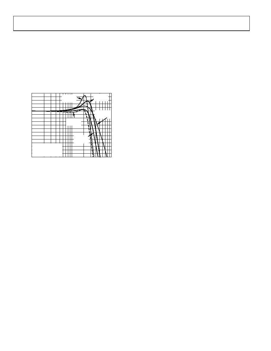
Figure 63. Frequency Response for
Various Capacitive Load and Series Resistance
The Typical Performance Characteristics that illustrate transient
response vs. the capacitive load were generated using series
resistors in each output and a differential capacitive load.
Layout Considerations
Standard high speed PCB layout practices should be adhered to
when designing with the AD8139. A solid ground plane is
recommended, and good wideband power supply decoupling
networks should be placed as close as possible to the supply pins.
To minimize stray capacitance at the summing nodes, the
copper in all layers under all traces and pads that connect to
the summing nodes should be removed. Small amounts of stray
summing-node capacitance cause peaking in the frequency
response, and large amounts can cause instability. If some stray
summing-node capacitance is unavoidable, its effects can be
compensated for by placing small capacitors across the feedback
resistors.
Terminating a Single-Ended Input
Controlled impedance interconnections are used in most
high speed signal applications, and they require at least one
line termination. In analog applications, a matched resistive
termination is generally placed at the load end of the line. This
section deals with how to properly terminate a single-ended
input to the AD8139.
The input resistance presented by the AD8139 input circuitry is
seen in parallel with the termination resistor, and its loading
effect must be taken into account. The Thevenin equivalent
circuit of the driver, its source resistance, and the termination
resistance must all be included in the calculation as well. An
exact solution to the problem requires the solution of several
simultaneous algebraic equations and is beyond the scope of
this data sheet. An iterative solution is also possible and simpler,
especially considering the fact that standard 1% resistor values
are generally used.
Figure 64 shows the AD8139 in a unity-gain configuration
driving the AD6645, which is a 14-bit, high speed ADC, and
with the following discussion, provides a good example of how
to provide a proper termination in a 50 Ω environment.
The termination resistor, RT, in parallel with the 268 Ω input
resistance of the AD8139 circuit (calculated using Equation 19),
yields an overall input resistance of 50 Ω that is seen by the
signal source. To have matched feedback loops, each loop must
have the same RG if they have the same RF. In the input (upper)
loop, RG is equal to the 200 Ω resistor in series with the (+)
input plus the parallel combination of RT and the source
resistance of 50 Ω. In the upper loop, RG is therefore equal to
228 Ω. The closest standard 1% value to 228 Ω is 226 Ω and is
used for RG in the lower loop. Greater accuracy could be
achieved by using two resistors in series to obtain a resistance
closer to 228 Ω.
Things get more complicated when it comes to determining
the feedback resistor values. The amplitude of the signal source
generator VS is two times the amplitude of its output signal
when terminated in 50 Ω. Therefore, a 2 V p-p terminated
amplitude is produced by a 4 V p-p amplitude from VS. The
Thevenin equivalent circuit of the signal source and RT must
be used when calculating the closed-loop gain, because in
the upper loop, RG is split between the 200 Ω resistor and
the Thevenin resistance looking back toward the source. The
Thevenin voltage of the signal source is greater than the signal
source output voltage when terminated in 50 Ω because RT
must always be greater than 50 Ω. In this case, RT is 61.9 Ω and
the Thevenin voltage and resistance are 2.2 V p-p and 28 Ω,
respectively. Now the upper input branch can be viewed as a
2.2 V p-p source in series with 228 Ω. Because this is a unity-
gain application, a 2 V p-p differential output is required, and
RF must therefore be 228 × (2/2.2) = 206 Ω. The closest
standard value to this is 205 Ω.
When generating the Typical Performance Characteristics data,
the measurements were calibrated to take the effects of the
terminations on the closed-loop gain into account.
相关PDF资料 |
PDF描述 |
|---|---|
| 69192-122HLF | BERGSTIK II DR STRAIGHT RET |
| 2089-250-BT1LF | SURGE ARRESTOR GDT 2500V AXIAL |
| 644861-3 | CONN HEADER VERT .100 3POS TIN |
| 69192-226HLF | BERGSTIK II DR STRAIGHT RET |
| 644861-2 | CONN HEADER VERT .100 2POS TIN |
相关代理商/技术参数 |
参数描述 |
|---|---|
| AD8139ACPZ-REEL7 | 功能描述:IC AMP DIFF R-R LN LDIST 8LFCSP RoHS:是 类别:集成电路 (IC) >> Linear - Amplifiers - Instrumentation 系列:- 标准包装:2,500 系列:- 放大器类型:通用 电路数:4 输出类型:- 转换速率:0.6 V/µs 增益带宽积:1MHz -3db带宽:- 电流 - 输入偏压:45nA 电压 - 输入偏移:2000µV 电流 - 电源:1.4mA 电流 - 输出 / 通道:40mA 电压 - 电源,单路/双路(±):3 V ~ 32 V,±1.5 V ~ 16 V 工作温度:0°C ~ 70°C 安装类型:表面贴装 封装/外壳:14-TSSOP(0.173",4.40mm 宽) 供应商设备封装:14-TSSOP 包装:带卷 (TR) 其它名称:LM324ADTBR2G-NDLM324ADTBR2GOSTR |
| AD8139AR | 制造商:Analog Devices 功能描述: |
| AD8139ARD | 功能描述:IC AMP DIFF R-R LN LDIST 8SOIC RoHS:否 类别:集成电路 (IC) >> Linear - Amplifiers - Instrumentation 系列:- 标准包装:2,500 系列:Excalibur™ 放大器类型:J-FET 电路数:1 输出类型:- 转换速率:45 V/µs 增益带宽积:10MHz -3db带宽:- 电流 - 输入偏压:20pA 电压 - 输入偏移:490µV 电流 - 电源:1.7mA 电流 - 输出 / 通道:48mA 电压 - 电源,单路/双路(±):4.5 V ~ 38 V,±2.25 V ~ 19 V 工作温度:-40°C ~ 85°C 安装类型:表面贴装 封装/外壳:8-SOIC(0.154",3.90mm 宽) 供应商设备封装:8-SOIC 包装:带卷 (TR) |
| AD8139ARD-EBZ | 功能描述:BOARD EVAL FOR AD8139ARD RoHS:是 类别:编程器,开发系统 >> 评估板 - 运算放大器 系列:- 产品培训模块:Lead (SnPb) Finish for COTS Obsolescence Mitigation Program 标准包装:1 系列:- |
| AD8139ARD-REEL | 功能描述:IC AMP DIFF R-R LN LDIST 8SOIC RoHS:否 类别:集成电路 (IC) >> Linear - Amplifiers - Instrumentation 系列:- 标准包装:50 系列:- 放大器类型:J-FET 电路数:2 输出类型:- 转换速率:3.5 V/µs 增益带宽积:1MHz -3db带宽:- 电流 - 输入偏压:30pA 电压 - 输入偏移:2000µV 电流 - 电源:200µA 电流 - 输出 / 通道:- 电压 - 电源,单路/双路(±):7 V ~ 36 V,±3.5 V ~ 18 V 工作温度:0°C ~ 70°C 安装类型:通孔 封装/外壳:8-DIP(0.300",7.62mm) 供应商设备封装:8-PDIP 包装:管件 |
发布紧急采购,3分钟左右您将得到回复。