- 您现在的位置:买卖IC网 > PDF目录10113 > AD8143ACPZ-REEL (Analog Devices Inc)IC RECEIVER TRIPLE DIFF 32LFCSP PDF资料下载
参数资料
| 型号: | AD8143ACPZ-REEL |
| 厂商: | Analog Devices Inc |
| 文件页数: | 24/24页 |
| 文件大小: | 0K |
| 描述: | IC RECEIVER TRIPLE DIFF 32LFCSP |
| 标准包装: | 5,000 |
| 类型: | 接收器 |
| 驱动器/接收器数: | 0/3 |
| 规程: | 以太网 |
| 电源电压: | 4.5 V ~ 24 V |
| 安装类型: | 表面贴装 |
| 封装/外壳: | 32-VFQFN 裸露焊盘,CSP |
| 供应商设备封装: | 32-LFCSP-VQ |
| 包装: | 带卷 (TR) |
AD8143
Rev. 0 | Page 9 of 24
ABSOLUTE MAXIMUM RATINGS
Table 4.
Parameter
Rating
Supply Voltage
24 V
Power Dissipation
See Figure 2
Storage Temperature Range
–65°C to +125°C
Operating Temperature Range
–40°C to +85°C
Lead Temperature Range (Soldering 10 sec)
300°C
Junction Temperature
150°C
Stresses above those listed under Absolute Maximum Ratings
may cause permanent damage to the device. This is a stress
rating only; functional operation of the device at these or any
other conditions above those indicated in the operational
section of this specification is not implied. Exposure to absolute
maximum rating conditions for extended periods may affect
device reliability.
THERMAL RESISTANCE
θJA is specified for the worst-case conditions, that is, θJA is
specified for a device soldered in the circuit board with its
exposed paddle soldered to a pad on the PCB surface which is
thermally connected to a copper plane.
Table 5. Thermal Resistance
Package Type
θJA
θJC
Unit
5 mm × 5 mm, 32-Lead LFCSP
45
7
°C/W
Maximum Power Dissipation
The maximum safe power dissipation in the AD8143 package is
limited by the associated rise in junction temperature (TJ) on
the die. At approximately 150°C, which is the glass transition
temperature, the plastic changes its properties. Even temporarily
exceeding this temperature limit can change the stresses that the
package exerts on the die, permanently shifting the parametric
performance of the AD8143. Exceeding a junction temperature
of 150°C for an extended period can result in changes in the
silicon devices potentially causing failure.
The power dissipated in the package (PD) is the sum of the
quiescent power dissipation and the power dissipated in the
package due to the load drive for all outputs. The quiescent
power is the voltage between the supply pins (VS) times the
quiescent current (IS). The power dissipated due to the load
drive depends upon the particular application. For each output,
the power due to load drive is calculated by multiplying the load
current by the associated voltage drop across the device. The
power dissipated due to all of the loads is equal to the sum of
the power dissipation due to each individual load. RMS voltages
and currents must be used in these calculations.
Airflow increases heat dissipation, effectively reducing θJA. In
addition, more metal directly in contact with the package leads
from metal traces, through-holes, ground, and power planes
reduces the θJA. The exposed paddle on the underside of the
package must be soldered to a pad on the PCB surface which is
thermally connected to a copper plane to achieve the specified θJA.
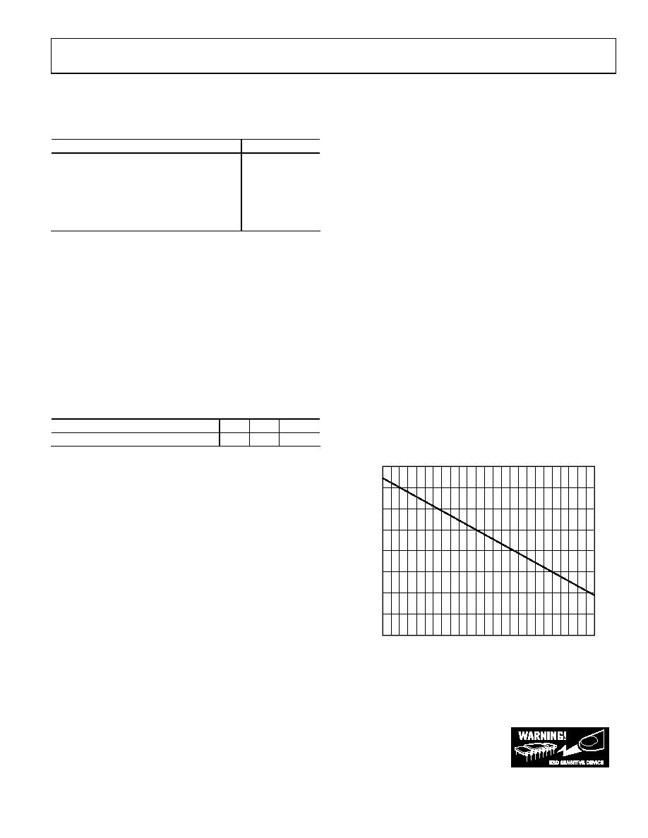
Figure 2 shows the maximum safe power dissipation in the
package vs. the ambient temperature for the 32-lead LFCSP
(45°C/W) on a JEDEC standard 4-layer board with the underside
paddle soldered to a pad which is thermally connected to a PCB
plane. Extra thermal relief is required for operation at high
supply voltages. See the Applications section for details. θJA
values are approximations.
0.5
1.0
1.5
2.0
2.5
3.0
3.5
4.0
4.5
–40
–200
20
406080
AMBIENT TEMPERATURE (°C)
MAXIMUM
PO
WER
DISSIPATIO
N
(W)
05538-
056
Figure 2. Maximum Power Dissipation vs. Temperature for a 4-Layer Board
ESD CAUTION
ESD (electrostatic discharge) sensitive device. Electrostatic charges as high as 4000 V readily accumulate on
the human body and test equipment and can discharge without detection. Although this product features
proprietary ESD protection circuitry, permanent damage may occur on devices subjected to high energy
electrostatic discharges. Therefore, proper ESD precautions are recommended to avoid performance
degradation or loss of functionality.
相关PDF资料 |
PDF描述 |
|---|---|
| LTC1383CN | IC TXRX 5V RS232 LOW PWR 16-DIP |
| VI-2NV-MX-F1 | CONVERTER MOD DC/DC 5.8V 75W |
| ADM2209EARU-REEL | IC TXRX6/10 RS-232 12V 38TSSOP |
| AD7701AN | IC ADC 16BIT LC2MOS 20-DIP |
| MS3102R36-4S | CONN RCPT 3POS BOX MNT W/SCKT |
相关代理商/技术参数 |
参数描述 |
|---|---|
| AD8143ACPZ-REEL7 | 功能描述:IC RECEIVER TRIPLE DIFF 32LFCSP RoHS:是 类别:集成电路 (IC) >> 接口 - 驱动器,接收器,收发器 系列:- 标准包装:27 系列:- 类型:收发器 驱动器/接收器数:3/3 规程:RS232,RS485 电源电压:4.75 V ~ 5.25 V 安装类型:表面贴装 封装/外壳:28-SOIC(0.295",7.50mm 宽) 供应商设备封装:28-SOIC 包装:管件 |
| AD8145 | 制造商:AD 制造商全称:Analog Devices 功能描述:High Speed, Triple Differential Receiver with Comparators |
| AD8145WYCPZ-R7 | 功能描述:IC RECEIVER TRIPLE DIFF 32LFCSP RoHS:是 类别:集成电路 (IC) >> 接口 - 驱动器,接收器,收发器 系列:- 标准包装:27 系列:- 类型:收发器 驱动器/接收器数:3/3 规程:RS232,RS485 电源电压:4.75 V ~ 5.25 V 安装类型:表面贴装 封装/外壳:28-SOIC(0.295",7.50mm 宽) 供应商设备封装:28-SOIC 包装:管件 |
| AD8145WYCPZ-R72 | 制造商:AD 制造商全称:Analog Devices 功能描述:High Speed, Triple Differential Receiver with Comparators |
| AD8145YCPZ-R2 | 制造商:Analog Devices 功能描述:Video Amp Triple 制造商:Analog Devices 功能描述:COMPARATOR TRIPLE 5.5V/11V 32LFCSP EP - Tape and Reel 制造商:Analog Devices 功能描述:HIGH SPEED TRIPLE RECEIVER 制造商:Analog Devices 功能描述:Difference And Buffer Amplifier IC 制造商:Analog Devices 功能描述:RECEIVER DIFFERENTIAL TRIPLE SMD 制造商:Analog Devices 功能描述:RECEIVER, DIFFERENTIAL, TRIPLE, SMD |
发布紧急采购,3分钟左右您将得到回复。