- 您现在的位置:买卖IC网 > PDF目录8571 > AD8148ACPZ-R2 (Analog Devices Inc)IC DRIVER TRPL DIFF VID 24LFCSP PDF资料下载
参数资料
| 型号: | AD8148ACPZ-R2 |
| 厂商: | Analog Devices Inc |
| 文件页数: | 13/24页 |
| 文件大小: | 0K |
| 描述: | IC DRIVER TRPL DIFF VID 24LFCSP |
| 标准包装: | 1 |
| 应用: | 差分 |
| 输出类型: | 差分 |
| 电路数: | 3 |
| -3db带宽: | 900MHz |
| 转换速率: | 3000 V/µs |
| 电流 - 电源: | 62.5mA |
| 电流 - 输出 / 通道: | 87mA |
| 电压 - 电源,单路/双路(±): | 4.5 V ~ 11 V,±2.25 V ~ 5.5 V |
| 安装类型: | 表面贴装 |
| 封装/外壳: | 24-VFQFN 裸露焊盘,CSP |
| 供应商设备封装: | 24-LFCSP-VQ(4x4) |
| 包装: | 标准包装 |
| 产品目录页面: | 765 (CN2011-ZH PDF) |
| 其它名称: | AD8148ACPZ-R2DKR |
AD8146/AD8147/AD8148
Data Sheet
Rev. B | Page 20 of 24
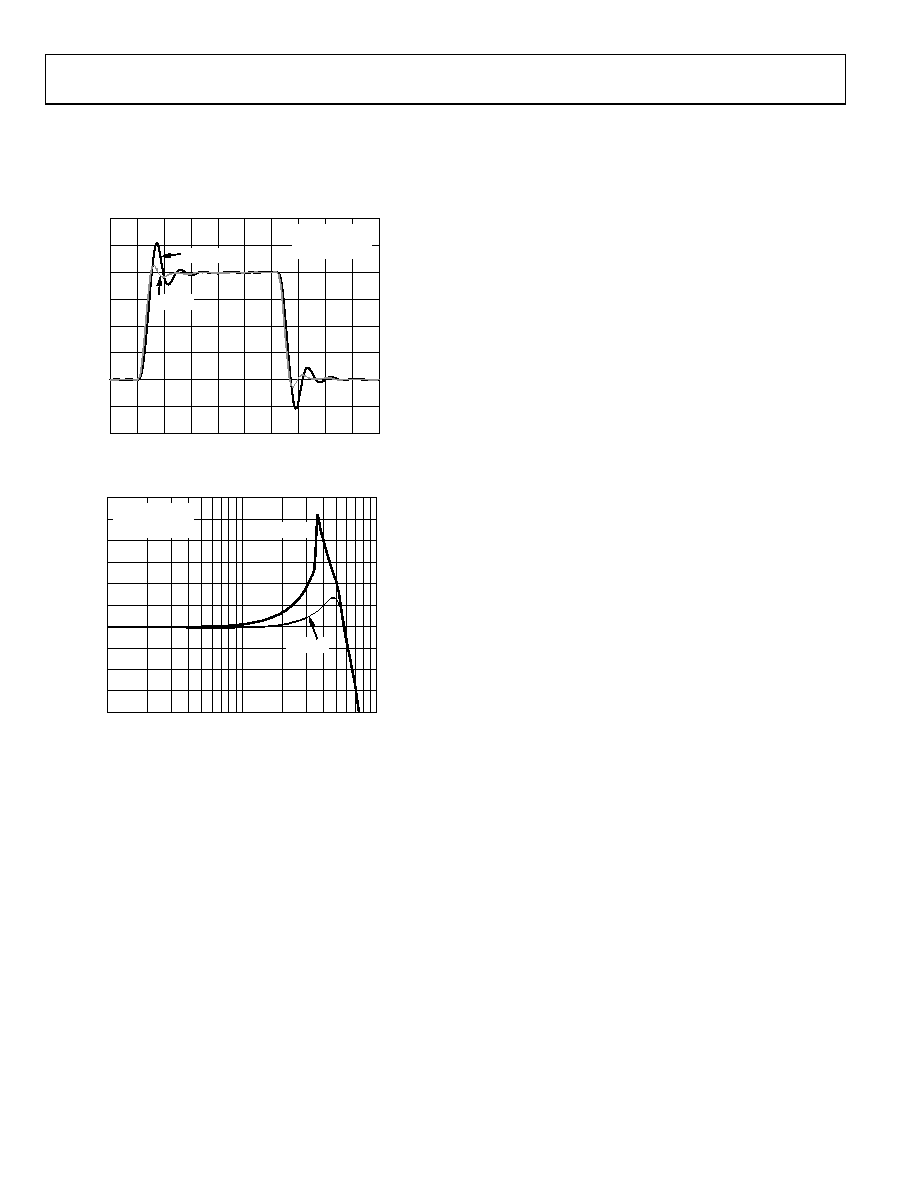
Under no circumstances should capacitance be intentionally
added to an output to introduce frequency domain peaking.
Figure 36 and Figure 37 illustrate how adding just 5 pF of
excessive load capacitance influences time and frequency
domain responses.
2.0
–2.0
0
20
TIME (ns)
VO
L
T
A
G
E
(V)
1.5
1.0
0.5
0
–0.5
–1.0
–1.5
2
4
6
8
10
12
14
16
18
VS = ±5V
RL, dm = 200Ω
VOUT, dm = 2V p-p
CL = 5pF
CL = 0pF
09327-
031
Figure 36. Large Signal Transient Responses at Various Capacitive Loads
12
2
10
1000
FREQUENCY (MHz)
G
AI
N
(
d
B)
100
11
10
9
8
7
6
5
4
3
VS = ±5V
RL, dm = 200Ω
VOUT, dm = 2V p-p
CL = 5pF
CL = 0pF
09327-
032
Figure 37. Large Signal Frequency Responses at Various Capacitive Loads
While high frequency peaking is desirable in some cable
equalization applications, it should be implemented using
methods that do not compromise the stability of the driver and
that do not depend on amplifier parasitic elements. The parasitic
elements are affected by process variations and cannot be
depended upon for circuit designs. The amplifier may break
into oscillation when excess load capacitance is intentionally
added. For more information on this topic, see the Adding Pre-
Emphasis to the section for a description on how to introduce a
controlled amount of pre-emphasis for 30 meters of UTP using
the AD8148.
ADDING PRE-EMPHASIS TO THE AD8148
UTP cables exhibit loss characteristics that are low pass in
nature and are exponential functions of the square root of the
frequency. Over wideband video bandwidths, the losses are
predominantly due to the skin effect, which causes the resistance of
the cable to increase with frequency. Even though the loss
characteristics are nonlinear, suitable linear networks can be
designed to approximately compensate for the losses.
Placing the compensation network at the transmitting end of
the cable is referred to as pre-emphasis, because the higher
frequencies are emphasized, or boosted, before they are sent, to
compensate for the low-pass response of the cable. Because the
higher frequencies experience more loss than the lower frequencies
as they pass through the cable, the high and low frequencies
arrive at approximately the same level and at the end of the cable
when a properly designed pre-emphasis network is used at the
transmitter. The ideal cascaded frequency response of the pre-
emphasis network and the cable is therefore nominally flat.
Because the AD8148 has an internally set, closed-loop gain of 4
(12 dB), it is possible to reduce the gain at low frequencies using
external frequency selective components, then use these
components to provide increasing gain with increasing
frequency, back to a value close to 12 dB. These components, along
with the AD8148, form the pre-emphasis network. When properly
designed, the combined frequency response of the pre-emphasis
network and cable is approximately flat with a gain of 2 (6 dB).
Figure 38 illustrates how to construct a pre-emphasis network
using the AD8148 that compensates for 30 meters of UTP cable.
The network in the lower leg is required to match the transfer
function of the two feedback loops.
At dc, the capacitors are open circuits, and the network has a
gain of approximately 6.5 dB. (The additional 0.5 dB is added to
compensate for the cable flat loss that occurs at frequencies
below where the skin effect begins to take effect.) Moving up in
frequency, the 30 pF capacitor begins to take effect and introduces
a zero into the frequency response, causing the gain to increase
with frequency. Continuing to move up in frequency, the 30 pF
capacitor becomes an effective short, and the 487 resistor
goes in parallel with the 442 resistor, forming a pole in the
response. Continuing to move up in frequency, the 18 pF
capacitor takes effect, introducing another zero, and causes
the gain to further increase with frequency until it becomes
an effective short, and the gain starts to flatten out until the
amplifier response begins to roll off. The gain does not reach
12 dB before the amplifier begins to roll off because the 12 dB
value is a high frequency asymptote. The pole and zero locations
cited in the previous discussion are qualitative, but the
discussion describes the basic principles involved with the
operation of the pre-emphasis network.
相关PDF资料 |
PDF描述 |
|---|---|
| AD7247JN | IC DAC 12BIT LC2MOS DUAL 24-DIP |
| VI-2NR-IV-F3 | CONVERTER MOD DC/DC 7.5V 150W |
| DS3514T+ | IC I2C GAMMA/VCOM BUFF 48-TQFN |
| MAX4029EUP+T | IC VIDEO MUX-AMP 20-TSSOP |
| VI-2NP-IV-F3 | CONVERTER MOD DC/DC 13.8V 150W |
相关代理商/技术参数 |
参数描述 |
|---|---|
| AD8148ACPZ-R7 | 功能描述:IC DRIVER TRIPLE DIFF 24-LFCSP RoHS:是 类别:集成电路 (IC) >> 线性 - 放大器 - 视频放大器和频缓冲器 系列:- 标准包装:1,000 系列:- 应用:驱动器 输出类型:差分 电路数:3 -3db带宽:350MHz 转换速率:1000 V/µs 电流 - 电源:14.5mA 电流 - 输出 / 通道:60mA 电压 - 电源,单路/双路(±):5 V ~ 12 V,±2.5 V ~ 6 V 安装类型:表面贴装 封装/外壳:20-VFQFN 裸露焊盘 供应商设备封装:20-QFN 裸露焊盘(4x4) 包装:带卷 (TR) |
| AD8148ACPZ-RL | 功能描述:IC DRIVER TRIPLE DIFF 24-LFCSP RoHS:是 类别:集成电路 (IC) >> 线性 - 放大器 - 视频放大器和频缓冲器 系列:- 标准包装:1,000 系列:- 应用:驱动器 输出类型:差分 电路数:3 -3db带宽:350MHz 转换速率:1000 V/µs 电流 - 电源:14.5mA 电流 - 输出 / 通道:60mA 电压 - 电源,单路/双路(±):5 V ~ 12 V,±2.5 V ~ 6 V 安装类型:表面贴装 封装/外壳:20-VFQFN 裸露焊盘 供应商设备封装:20-QFN 裸露焊盘(4x4) 包装:带卷 (TR) |
| AD815 | 制造商:未知厂家 制造商全称:未知厂家 功能描述:SILICON DUAL DIFFERNTIAL AMPLIFIER TRANSISTORS |
| AD815_05 | 制造商:AD 制造商全称:Analog Devices 功能描述:High Output Current Differential Driver |
| AD8150 | 制造商:AD 制造商全称:Analog Devices 功能描述:33 x 17, 1.5 Gbps Digital Crosspoint Switch |
发布紧急采购,3分钟左右您将得到回复。