- 您现在的位置:买卖IC网 > PDF目录378276 > AD8152 (Analog Devices, Inc.) 34 x 34, 3.2 Gbps Asynchronous Digital Crosspoint Switch PDF资料下载
参数资料
| 型号: | AD8152 |
| 厂商: | Analog Devices, Inc. |
| 英文描述: | 34 x 34, 3.2 Gbps Asynchronous Digital Crosspoint Switch |
| 中文描述: | 34 × 34,3.2 Gbps的异步数字交叉点开关 |
| 文件页数: | 19/32页 |
| 文件大小: | 1351K |
| 代理商: | AD8152 |
第1页第2页第3页第4页第5页第6页第7页第8页第9页第10页第11页第12页第13页第14页第15页第16页第17页第18页当前第19页第20页第21页第22页第23页第24页第25页第26页第27页第28页第29页第30页第31页第32页
REV. A
AD8152
–19–
is powered down. Thus, the total number of active inputs will
affect the total power consumption.
The core of the device performs the crosspoint switching function.
It draws a fixed quiescent current whenever the AD8152 is
powered from VCC to VEE.
An output predriver section draws a current that is proportional
to the programmed output current, I
OUT
. This current always
flows from VCC to VEE. It is treated separately from the output
current, which flows from VTTO, and might not be the same
voltage as VCC.
The final section is the outputs. For an individual output, the
programmed output current will flow through two separate paths.
One is the on-chip termination resistor, and the other is the
transmission line and the destination termination resistor. The
nominal parallel impedance of these two paths is 25
W
. The sum
INPUT
TERMINATIONS
INPUTS
OUT-
PUTS
VTTI
VEE
VCC
VTTO
VTT
50
50
INP
INN
50
50
DRIVEN DEVICE
TERMINATIONS
I
OUT
OUTP
OUTN
50
50
OUTPUT TERMINATIONS
I
OUT
2
V
OL
= V
TTO
– (I
OUT
25 )
OPTIONAL COUPLING CAPACITORS
SWITCH
MATRIX
OUTPUT
PRE-
DRIVER
I = 32mA
I = .25 I
OUT
50
P =
P =
(V
indiffrms
)
2
100
(V
OL
) (I
OUT
)
P =
I = 2mA
PER
ACTIVE
INPUT
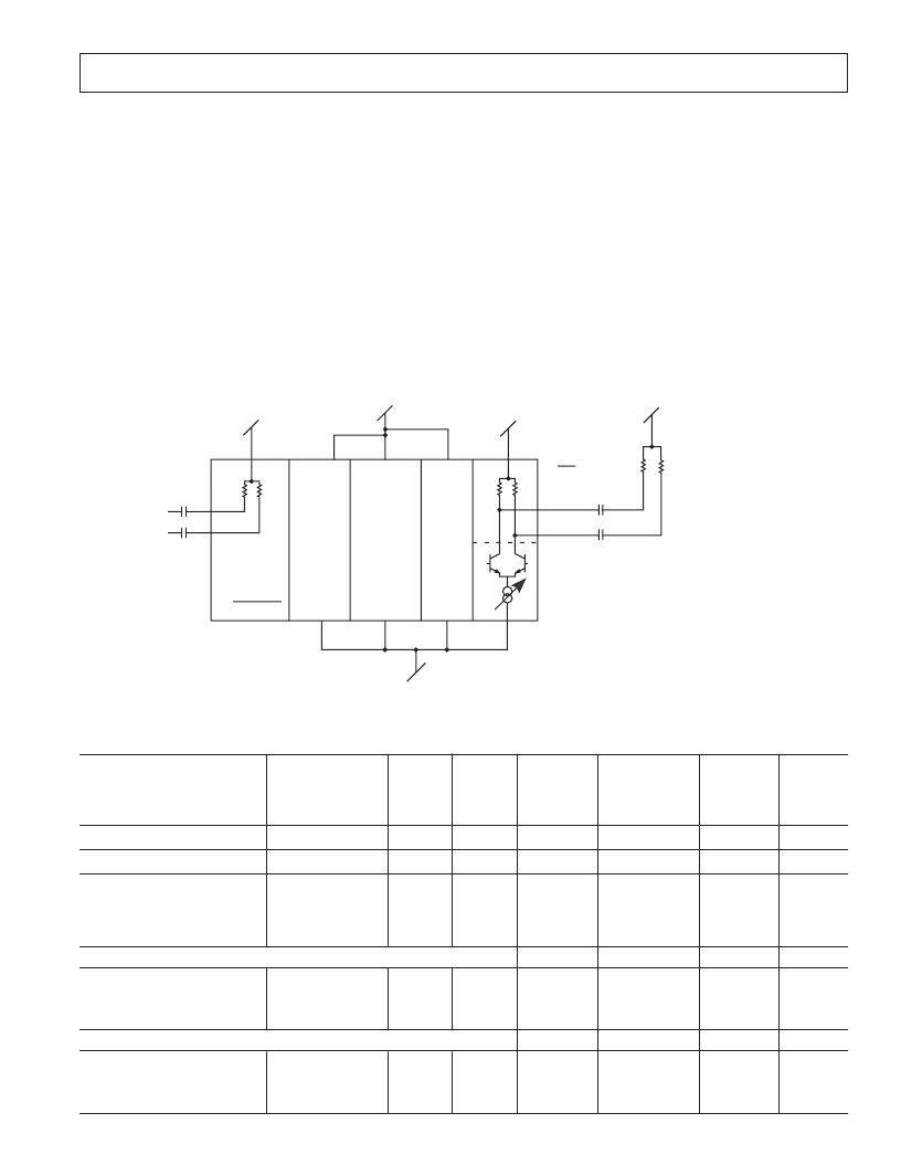
Figure 9. Power Consumption Block Diagram
Table X. Power Consumption
Output
Switch +
Current
Source
Input
Termination
Resistors
Output
Termination
Resistors
Input
Stage
Output
Predriver
Total
Power
Core
Quiescent Current
32 mA
Current per Active Channel
V
IN
/
(R
TERMINATION
)
2 mA
0.25
¥
I
OUT
0.5
¥
I
OUT
I
OUT
Current per Active
Channel
for Differential
V
IN
= 800 mV p-p Sine
V
OUT
= 800 mV p-p
2.5 V Operation
(
VCC – VEE =
2.5 V
,
VTTO = 2.5 V, I
OUT
= 16 mA)
Per Channel Power
3.2 mW
Power for All Channels Active
108.8 mW
Percentage of Total Power
5%
3.3 V Operation
(
VCC –
VEE =
3.3 V,
VTTO =
3.3
V, I
OUT
= 16 mA)
Per Channel Power
3.2 mW
Power for All Channels Active
108.8 mW
Percentage of Total Power
4%
566 mV rms/100
= 5.66 mA
2 mA
4 mA
4 mA
8 mA
16 mA
5 mW
170 mW
8%
10 mW
340 mW
17%
8 mW
272 mW
13.6%
33.6 mW
1.03 W
51%
80 mW
4%
2.0 W
6.6 mW
224 mW
9%
13.2 mW
449 mW
17%
8 mW
272 mW
10%
46.4 mW
1.47 W
56%
106 mW
4%
2.63 W
AD8152 POWER CONSUMPTION
There are several sections of the AD8152 that draw varying
power depending on the supply voltages, the type of I/O coupling
used, and the status of the AD8152 operation. Figure 9 shows a
block diagram of these sections. These are described briefly below
and then in detail later in the data sheet. Table X summarizes the
power consumption of each section and is a useful guide as the
following sections are reviewed.
The first section is the input termination resistors. The power
dissipated in the termination resistors is the result of their being
driven by the respective driving stage. Also, there might be dc power
dissipated in the input termination resistors if the inputs are
dc-coupled and the driving source reference is a dc voltage that is
not equal to VTTI.
In the next section, the active part of the input stages, each input
is powered only when it is selected. If an input is not selected, it
相关PDF资料 |
PDF描述 |
|---|---|
| AD8152-EVAL | 34 x 34, 3.2 Gbps Asynchronous Digital Crosspoint Switch |
| AD8152JBP | 34 x 34, 3.2 Gbps Asynchronous Digital Crosspoint Switch |
| AD82550A | Stereo Digital Audio Amplifier with Headphone Driver |
| AD82550A-CG | Stereo Digital Audio Amplifier with Headphone Driver |
| AD82551A | Stereo Digital Audio Amplifier with Headphone Driver |
相关代理商/技术参数 |
参数描述 |
|---|---|
| AD8152-EVAL | 制造商:Analog Devices 功能描述:EVAL KIT FOR ASYNCH DGTL CROSSPOINT SWIT - Bulk |
| AD8152JBP | 功能描述:IC CROSSPOINT SWIT 34X34 256BGA RoHS:否 类别:集成电路 (IC) >> 接口 - 模拟开关,多路复用器,多路分解器 系列:XStream™ 其它有关文件:STG4159 View All Specifications 标准包装:5,000 系列:- 功能:开关 电路:1 x SPDT 导通状态电阻:300 毫欧 电压电源:双电源 电压 - 电源,单路/双路(±):±1.65 V ~ 4.8 V 电流 - 电源:50nA 工作温度:-40°C ~ 85°C 安装类型:表面贴装 封装/外壳:7-WFBGA,FCBGA 供应商设备封装:7-覆晶 包装:带卷 (TR) |
| AD8152JBPZ | 功能描述:IC CROSSPOINT SWIT 34X34 256BGA RoHS:是 类别:集成电路 (IC) >> 接口 - 模拟开关,多路复用器,多路分解器 系列:XStream™ 应用说明:Ultrasound Imaging Systems Application Note 产品培训模块:Lead (SnPb) Finish for COTS Obsolescence Mitigation Program 标准包装:250 系列:- 功能:开关 电路:单刀单掷 导通状态电阻:48 欧姆 电压电源:单电源 电压 - 电源,单路/双路(±):2.7 V ~ 5.5 V 电流 - 电源:5µA 工作温度:0°C ~ 70°C 安装类型:表面贴装 封装/外壳:48-LQFP 供应商设备封装:48-LQFP(7x7) 包装:托盘 |
| AD8153 | 制造商:AD 制造商全称:Analog Devices 功能描述:3.2 Gbps Single Buffered Mux/Demux Switch |
| AD8153_07 | 制造商:AD 制造商全称:Analog Devices 功能描述:3.2 Gbps Single Buffered Mux/Demux Switch |
发布紧急采购,3分钟左右您将得到回复。