- 您现在的位置:买卖IC网 > PDF目录373939 > AD815 (Analog Devices, Inc.) High Output Current Differential Driver(高输出电流差分驱动器) PDF资料下载
参数资料
| 型号: | AD815 |
| 厂商: | Analog Devices, Inc. |
| 英文描述: | High Output Current Differential Driver(高输出电流差分驱动器) |
| 中文描述: | 高输出电流差动驱动器(高输出电流差分驱动器) |
| 文件页数: | 10/16页 |
| 文件大小: | 320K |
| 代理商: | AD815 |
AD815
REV. A
–10–
Choice of Feedback and Gain Resistors
T he fine scale gain flatness will, to some extent, vary with
feedback resistance. It therefore is recommended that once
optimum resistor values have been determined, 1% tolerance
values should be used if it is desired to maintain flatness over a
wide range of production lots. T able I shows optimum values
for several useful configurations. T hese should be used as
starting point in any application.
T able I. Resistor Values
R
F
(
V
)
R
G
(
V
)
G =
+1
–1
+2
+5
+10
562
499
499
499
1K
`
499
499
125
110
PRINT E D CIRCUIT BOARD LAY OUT
C ONSIDE RAT IONS
As to be expected for a wideband amplifier, PC board parasitics
can affect the overall closed-loop performance. Of concern are
stray capacitances at the output and the inverting input nodes. If
a ground plane is to be used on the same side of the board as
the signal traces, a space (5 mm min) should be left around the
signal lines to minimize coupling.
POWE R SUPPLY BY PASSING
Adequate power supply bypassing can be critical when optimizing
the performance of a high frequency circuit. Inductance in the
power supply leads can form resonant circuits that produce
peaking in the amplifier’s response. In addition, if large current
transients must be delivered to the load, then bypass capacitors
(typically greater than 1
μ
F) will be required to provide the best
settling time and lowest distortion. A parallel combination of
10.0
μ
F and 0.1
μ
F is recommended. Under some low fre-
quency applications, a bypass capacitance of greater than 10
μ
F
may be necessary. Due to the large load currents delivered by
the AD815, special consideration must be given to careful by-
passing. T he ground returns on both supply bypass capacitors
as well as signal common must be “star” connected as shown in
Figure 41.
R
F
R
G
(OPTIONAL)
R
F
+V
S
+OUT
–OUT
–V
S
+IN
–IN
Figure 41. Signal Ground Connected in “ Star”
Configuration
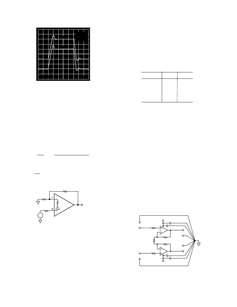
1V
20ns
SIDE B
SIDE A
G = –1
R
F
= 562
R
L
= 100
Figure 39. 4 V Step Response, G = –1
T HE ORY OF OPE RAT ION
T he AD815 is a dual current feedback amplifier with high
(500 mA) output current capability. Being a current feedback
amplifier, the AD815’s open-loop behavior is expressed as
transimpedance,
V
O
/
I
–IN
, or T
Z
. T he open-loop transimped-
ance behaves just as the open-loop voltage gain of a voltage
feedback amplifier, that is, it has a large dc value and decreases
at roughly 6 dB/octave in frequency.
Since R
IN
is proportional to 1/g
M
, the equivalent voltage gain is
just T
Z
×
g
M
, where the g
M
in question is the transconductance
of the input stage. Using this amplifier as a follower with gain,
Figure 40, basic analysis yields the following result:
V
O
V
IN
=
G
×
T
Z
S
( )
T
Z
S
( )
+
G
×
R
IN
+
R
F
where:
G
=
1
+
R
F
R
G
R
IN
= 1/
g
M
≈
25
R
IN
V
IN
R
F
V
OUT
R
G
R
N
Figure 40.
Recognizing that G
×
R
IN
<< R
F
for low gains, it can be seen to
the first order that bandwidth for this amplifier is independent
of gain (G).
Considering that additional poles contribute excess phase at
high frequencies, there is a minimum feedback resistance below
which peaking or oscillation may result. T his fact is used to
determine the optimum feedback resistance, R
F
. In practice
parasitic capacitance at the inverting input terminal will also add
phase in the feedback loop, so picking an optimum value for R
F
can be difficult.
Achieving and maintaining gain flatness of better than 0.1 dB at
frequencies above 10 MHz requires careful consideration of
several issues.
相关PDF资料 |
PDF描述 |
|---|---|
| AD816 | 500 mA Differential Driver & Dual Low Noise (VF) Amplifiers(500mA差分驱动器和双低噪电压反馈放大器) |
| AD8170AN | 250 MHz, 10 ns Switching Multiplexers w/Amplifier |
| AD8170AR | 250 MHz, 10 ns Switching Multiplexers w/Amplifier |
| AD8170-EB | 250 MHz, 10 ns Switching Multiplexers w/Amplifier |
| AD8170AR-REEL | 250 MHz, 10 ns Switching Multiplexers w/Amplifier |
相关代理商/技术参数 |
参数描述 |
|---|---|
| AD815_05 | 制造商:AD 制造商全称:Analog Devices 功能描述:High Output Current Differential Driver |
| AD8150 | 制造商:AD 制造商全称:Analog Devices 功能描述:33 x 17, 1.5 Gbps Digital Crosspoint Switch |
| AD8150AST | 制造商:Rochester Electronics LLC 功能描述:LQFP 1.5GBPS 33X17 DIGITAL CROSSPOINT SW - Tape and Reel 制造商:Analog Devices 功能描述:IC SWITCH CROSSPOINT |
| AD8150ASTZ | 功能描述:IC CROSSPOINT SWIT 33X17 184LQFP RoHS:是 类别:集成电路 (IC) >> 接口 - 模拟开关,多路复用器,多路分解器 系列:XStream™ 应用说明:Ultrasound Imaging Systems Application Note 产品培训模块:Lead (SnPb) Finish for COTS Obsolescence Mitigation Program 标准包装:250 系列:- 功能:开关 电路:单刀单掷 导通状态电阻:48 欧姆 电压电源:单电源 电压 - 电源,单路/双路(±):2.7 V ~ 5.5 V 电流 - 电源:5µA 工作温度:0°C ~ 70°C 安装类型:表面贴装 封装/外壳:48-LQFP 供应商设备封装:48-LQFP(7x7) 包装:托盘 |
| AD8150ASTZ | 制造商:Analog Devices 功能描述:IC DIGITAL CROSSPOINT SWITCH |
发布紧急采购,3分钟左右您将得到回复。