- 您现在的位置:买卖IC网 > PDF目录373939 > AD815AY (ANALOG DEVICES INC) High Output Current Differential Driver PDF资料下载
参数资料
| 型号: | AD815AY |
| 厂商: | ANALOG DEVICES INC |
| 元件分类: | 通用总线功能 |
| 英文描述: | High Output Current Differential Driver |
| 中文描述: | LINE DRIVER, PZFM15 |
| 文件页数: | 3/16页 |
| 文件大小: | 333K |
| 代理商: | AD815AY |
AD815
REV. B
–3–
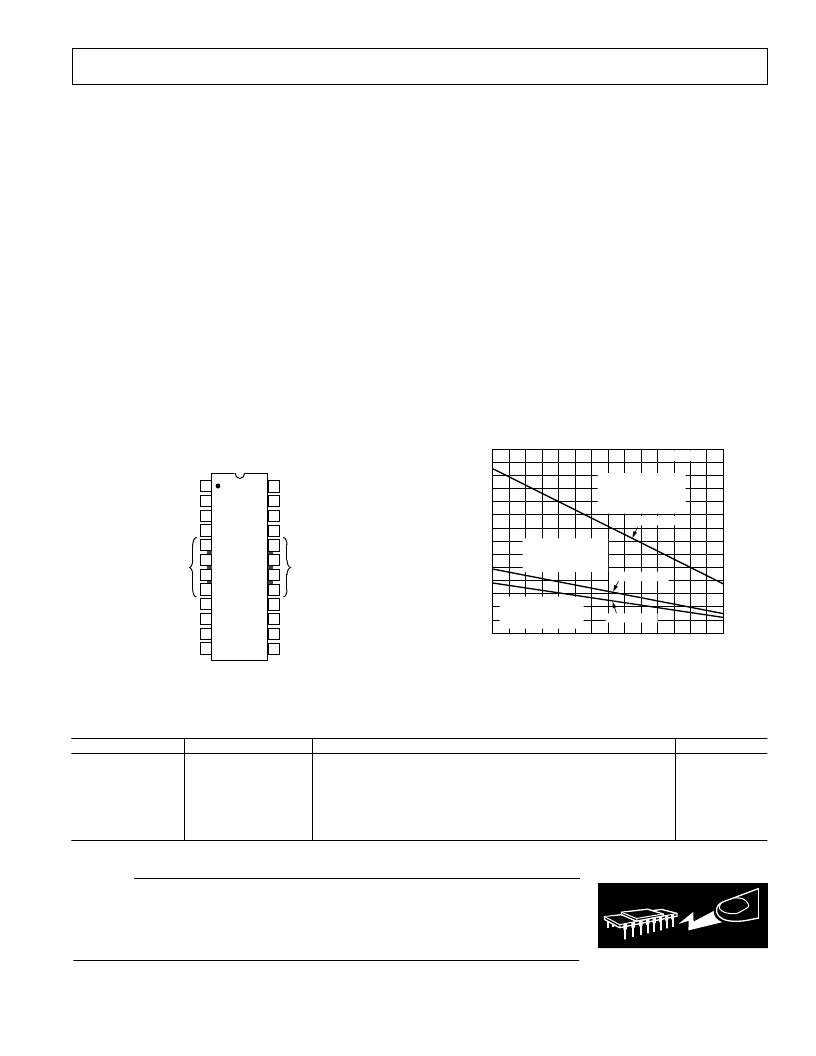
MAXIMUM POWER DISSIPATION
The maximum power that can be safely dissipated by the AD815
is limited by the associated rise in junction temperature. The
maximum safe junction temperature for the plastic encapsulated
parts is determined by the glass transition temperature of the
plastic, about 150
°
C. Exceeding this limit temporarily may
cause a shift in parametric performance due to a change in the
stresses exerted on the die by the package. Exceeding a junction
temperature of 175
°
C for an extended period can result in
device failure.
The AD815 has thermal shutdown protection, which guarantees
that the maximum junction temperature of the die remains below a
safe level, even when the output is shorted to ground. Shorting
the output to either power supply will result in device failure.
To ensure proper operation, it is important to observe the
derating curves and refer to the section on power considerations.
It must also be noted that in high (noninverting) gain configurations
(with low values of gain resistor), a high level of input overdrive
can result in a large input error current, which may result in a
significant power dissipation in the input stage. This power
must be included when computing the junction temperature rise
due to total internal power.
AMBIENT TEMPERATURE –
8
C
14
7
4
–50
90
–40
M
–30 –20 –10
10
20 30
40
50 60
70 80
13
12
8
6
5
11
9
10
0
T
J
= 150
8
C
3
2
1
0
AD815 AVR, AY
θ
JA
= 41
8
C/W
(STILL AIR = 0FT/MIN)
NO HEAT SINK
θ
= 52
8
C/W
(STILL AIR = 0 FT/MIN)
NO HEAT SINK
AD815ARB-24
θ
JA
= 16
8
C/W
SOLDERED DOWN TO
COPPER HEAT SINK
(STILL AIR = 0FT/MIN)
AD815 AVR, AY
Plot of Maximum Power Dissipation vs. Temperature
ABSOLUTE MAXIMUM RATINGS
1
Supply Voltage . . . . . . . . . . . . . . . . . . . . . . . . . . .
±
18 V Total
Internal Power Dissipation
2
Plastic (Y and VR) . . 3.05 Watts (Observe Derating Curves)
Small Outline (RB) . . 2.4 Watts (Observe Derating Curves)
Input Voltage (Common Mode) . . . . . . . . . . . . . . . . . . . .
±
V
S
Differential Input Voltage . . . . . . . . . . . . . . . . . . . . . . . .
±
6 V
Output Short Circuit Duration
. . . . . . . . . . . . . . . . . . . . . . Observe Power Derating Curves
Can Only Short to Ground
Storage Temperature Range
Y, VR and RB Package . . . . . . . . . . . . . . . –65
°
C to +125
°
C
Operating Temperature Range
AD815A . . . . . . . . . . . . . . . . . . . . . . . . . . . –40
°
C to +85
°
C
Lead Temperature Range (Soldering, 10 sec) . . . . . . . +300
°
C
NOTES
1
Stresses above those listed under Absolute Maximum Ratings may cause perma-
nent damage to the device. This is a stress rating only; functional operation of the
device at these or any other conditions above those indicated in the operational
section of this specification is not implied. Exposure to absolute maximum rating
conditions for extended periods may affect device reliability.
2
Specification is for device in free air with 0 ft/min air flow: 15-Lead Through-Hole
and Surface Mount:
θ
JA
= 41
°
C/W; 24-Lead Surface Mount:
θ
JA
= 52
°
C/W.
PIN CONFIGURATION
24-Lead Thermally-Enhanced SOIC (RB-24)
TOP VIEW
(Not to Scale)
AD815
13
16
15
14
24
23
22
21
20
19
18
17
12
11
10
9
8
1
2
3
4
7
6
5
NC = NO CONNECT
NC
NC
NC
NC
NC
NC
NC
NC
+IN1
–IN1
–IN2
+IN2
OUT1
–V
S
OUT2
+V
S
*HEAT TABS ARE CONNECTED TO THE POSITIVE SUPPLY.
THERMAL
HEAT TABS
+V
S
*
THERMAL
HEAT TABS
+V
S
*
ORDERING GUIDE
Model
AD815ARB-24
AD815ARB-24-REEL
AD815AVR
AD815AY
AD815AYS
AD815-EB
Temperature Range
–40
°
C to +85
°
C
–40
°
C to +85
°
C
–40
°
C to +85
°
C
–40
°
C to +85
°
C
–40
°
C to +85
°
C
Package Description
24-Lead Thermally Enhanced SOIC
24-Lead Thermally Enhanced SOIC
15-Lead Surface Mount DDPAK
15-Lead Through-Hole SIP with Staggered Leads and 90
°
Lead Form
15-Lead Through-Hole SIP with Staggered Leads and Straight Lead Form
Evaluation Board
Package Option
RB-24
RB-24
VR-15
Y-15
YS-15
CAUTION
ESD (electrostatic discharge) sensitive device. Electrostatic charges as high as 4000 V readily
accumulate on the human body and test equipment and can discharge without detection.
Although the AD815 features proprietary ESD protection circuitry, permanent damage may
occur on devices subjected to high energy electrostatic discharges. Therefore, proper ESD
precautions are recommended to avoid performance degradation or loss of functionality.
WARNING!
ESD SENSITIVE DEVICE
相关PDF资料 |
PDF描述 |
|---|---|
| AD815AYS | High Output Current Differential Driver |
| AD815 | High Output Current Differential Driver(高输出电流差分驱动器) |
| AD816 | 500 mA Differential Driver & Dual Low Noise (VF) Amplifiers(500mA差分驱动器和双低噪电压反馈放大器) |
| AD8170AN | 250 MHz, 10 ns Switching Multiplexers w/Amplifier |
| AD8170AR | 250 MHz, 10 ns Switching Multiplexers w/Amplifier |
相关代理商/技术参数 |
参数描述 |
|---|---|
| AD815AYS | 制造商:Rochester Electronics LLC 功能描述:- Bulk |
| AD815AYS-15 | 制造商:Analog Devices 功能描述:OP AMP DUAL GP 18V 15SIP - Bulk |
| AD815-EB | 制造商:Analog Devices 功能描述: |
| AD816 | 制造商:未知厂家 制造商全称:未知厂家 功能描述:SILICON DUAL DIFFERNTIAL AMPLIFIER TRANSISTORS |
发布紧急采购,3分钟左右您将得到回复。