- 您现在的位置:买卖IC网 > PDF目录373939 > AD816 (Analog Devices, Inc.) 500 mA Differential Driver & Dual Low Noise (VF) Amplifiers(500mA差分驱动器和双低噪电压反馈放大器) PDF资料下载
参数资料
| 型号: | AD816 |
| 厂商: | Analog Devices, Inc. |
| 英文描述: | 500 mA Differential Driver & Dual Low Noise (VF) Amplifiers(500mA差分驱动器和双低噪电压反馈放大器) |
| 中文描述: | 500毫安差分驱动器 |
| 文件页数: | 11/16页 |
| 文件大小: | 479K |
| 代理商: | AD816 |
AD816
REV. 0
–11–
Table I. Driver Resistor Values
R
F
(
V
)
R
G
(
V
)
G = +1
604
499
499
499
1k
∞
499
499
125
110
–1
+2
+5
+10
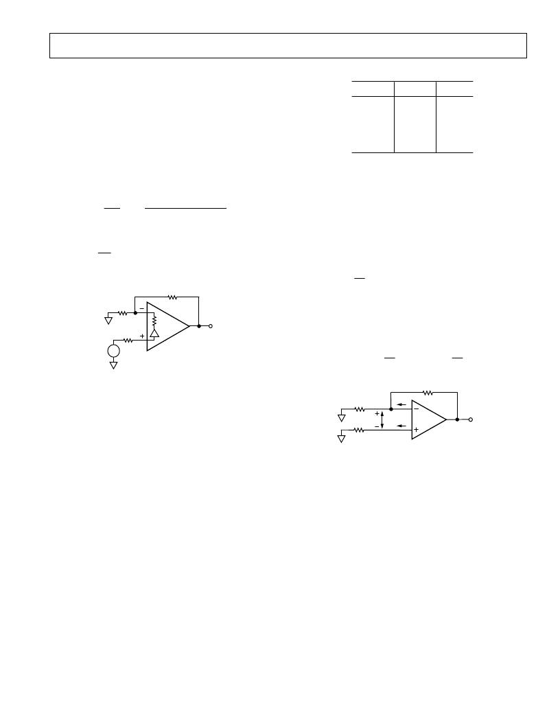
DRIVER DC ERRORS AND NOISE
There are three major noise and offset terms to consider in a
current feedback amplifier. For offset errors refer to the
equation below. For noise error the terms are root-sum-squared
to give a net output error. In the circuit below (Figure 43), they
are input offset (V
IO
) which appears at the output multiplied by
the noise gain of the circuit (1 + R
F
/R
G
), noninverting input
current (I
BN
×
R
N
) also multiplied by the noise gain, and the
inverting input current, which when divided between R
F
and R
G
and subsequently multiplied by the noise gain always appear at
the output as I
BI
×
R
F
. The input voltage noise of the AD816 is
less than 4 nV/
Hz
. At low gains, however, the inverting input
current noise times R
F
is the dominant noise source. Careful
layout and device matching contribute to better offset and drift.
The typical performance curves in conjunction with the
equations below can be used to predict the performance of the
AD816 in any application.
V
OUT
=
VIO
1
+
R
F
R
G
±
I
BN
R
N
1
+
R
F
R
G
±
I
BI
R
F
I
BI
I
BN
R
G
R
N
R
F
V
OUT
AD816
DRIVERS
VIO
Figure 43. Driver Output Offset Voltage
THEORY OF OPERATION (RECEIVER)
Each AD816 receiver is a wide band high performance
operational amplifier. It also provides a constant slew rate,
bandwidth and settling time over its entire specified temperature
range.
The AD816 receiver consists of a degenerated NPN differential
pair driving matched PNPs in a folded-cascode gain stage. The
output buffer stage employs emitter followers in a class AB
amplifier which deliver the necessary current to the load while
maintaining low levels of distortion.
A protection resistor in series with the noninverting input is
required in circuits where the input to the receiver could be
subject to transients on continuous overload voltages exceeding
the
±
6 V maximum differential limit. The resistor provides
protection for the input transistors, by limiting their maximum
base current.
THEORY OF OPERATION (DRIVER)
The AD816 driver is a dual current feedback amplifier with high
(500 mA) output current capability. Being a current feedback
amplifier, the AD816 driver’s open-loop behavior is expressed
as transimpedance,
V
O
/
I
–IN
, or T
Z
. The open-loop trans-
impedance behaves just as the open-loop voltage gain of a
voltage feedback amplifier, that is, it has a large dc value and
decreases at roughly 6 dB/octave in frequency.
Since R
IN
is proportional to 1/g
M
, the equivalent voltage gain is
just T
Z
×
g
M
, where the g
M
in question is the transconductance
of the input stage. Figure 42 shows the driver connected as a
follower with gain. Basic analysis yields the following results:
V
O
V
IN
=
G
×
T
Z
S
( )
T
Z
S
( )
+
G
×
R
IN
+
R
F
where:
G
=
1
+
R
F
R
G
R
IN
= 1/
g
M
≈
25
R
IN
V
IN
R
F
V
OUT
R
G
R
N
Figure 42. Current-Feedback Amplifier Operation
Recognizing that G
×
R
IN
<< R
F
for low gains, it can be seen to
the first order that bandwidth for this amplifier is independent
of gain (G).
Considering that additional poles contribute excess phase at
high frequencies, there is a minimum feedback resistance below
which peaking or oscillation may result. This fact is used to
determine the optimum feedback resistance, R
F
. In practice
parasitic capacitance at the inverting input terminal will also add
phase in the feedback loop so that picking an optimum value for
R
F
can be difficult.
Achieving and maintaining gain flatness of better than 0.1 dB at
frequencies above 10 MHz requires careful consideration of
several issues.
Choice of Feedback and Gain Resistors
The fine scale gain flatness will, to some extent, vary with
feedback resistance. It is therefore recommended that once
optimum resistor values have been determined, 1% tolerance
values should be used if it is desired to maintain flatness over a
wide range of production lots. Table I shows optimum values
for several useful gain configurations. These should be used as a
starting point in any application.
相关PDF资料 |
PDF描述 |
|---|---|
| AD8170AN | 250 MHz, 10 ns Switching Multiplexers w/Amplifier |
| AD8170AR | 250 MHz, 10 ns Switching Multiplexers w/Amplifier |
| AD8170-EB | 250 MHz, 10 ns Switching Multiplexers w/Amplifier |
| AD8170AR-REEL | 250 MHz, 10 ns Switching Multiplexers w/Amplifier |
| AD8174-EB | 250 MHz, 10 ns Switching Multiplexers w/Amplifier |
相关代理商/技术参数 |
参数描述 |
|---|---|
| AD816AVR | 制造商:Rochester Electronics LLC 功能描述:ADSL TRANSCEIVER - Bulk |
| AD816AY | 制造商:Rochester Electronics LLC 功能描述:ADSL TRANSCEIVER - Bulk |
| AD816AYR | 制造商:未知厂家 制造商全称:未知厂家 功能描述:Analog IC |
| AD816AYS | 制造商:Rochester Electronics LLC 功能描述:- Bulk |
发布紧急采购,3分钟左右您将得到回复。