- 您现在的位置:买卖IC网 > PDF目录373939 > AD8170-EB (Analog Devices, Inc.) 250 MHz, 10 ns Switching Multiplexers w/Amplifier PDF资料下载
参数资料
| 型号: | AD8170-EB |
| 厂商: | Analog Devices, Inc. |
| 英文描述: | 250 MHz, 10 ns Switching Multiplexers w/Amplifier |
| 中文描述: | 250兆赫,10 ns的开关多路复用器瓦特/放大器 |
| 文件页数: | 9/16页 |
| 文件大小: | 474K |
| 代理商: | AD8170-EB |
AD8170/AD8174
–9–
REV. 0
Equation 4 can be used to calculate expected gain error due to
the current feedback amplifier’s finite transimpedance and
common mode rejection. For low gains and recommended
feedback resistors, this will be typically less than 0.4%. For
most applications with gain greater than 1, the dominant source
of gain error will most likely be the ratio-match of the external
resistors. All of the dominant contributors to gain error are
associated with the buffer amplifier and external resistors.
These do not change as different channels are selected, so
channel-to-channel gain match of less than 0.05% is easily
attained.
G
=
1
+
R
F
R
G
R
T
R
T
+
R
IN
1
+
R
F
R
G
+
R
F
1
CMRR
[
]
(4)
↑
↑
Ideal Gain Error Terms
R
T
= Amplifier Transresistance = 600 k
R
IN
= Amplifier Input Resistance
100
CMRR
= Amplifier Common-Mode Rejection
–52 dB
Choice of External Resistors
The gain and bandwidth of the multiplexer are determined by
the closed-loop gain and bandwidth of the onboard current
feedback amplifier. These both may be customized by the
external resistor feedback network. Table III shows typical
bandwidths at some common closed loop gains for given
feedback and gain resistors (R
F
and R
G
, respectively).
The choice of R
F
is not critical unless the widest and flattest
frequency response must be maintained. The resistors recom-
mended in the table result in the widest 0.1 dB bandwidth with
the least peaking. 1% resistors are recommended for applications
requiring the best control of bandwidth. Packaging parasitics vary
between DIP and SOIC packages, which may result in a slightly
different resistor value for optimum frequency performance.
Wider bandwidths than those listed in the table can be attained
by reducing R
F
at the expense of increased peaking.
To estimate the –3 dB bandwidth for feedback resistors not
listed in Table III, the following single-pole model for the
current feedback amplifier may be used:
A
CL
=
G
1
+
sC
T
R
F
+
G
N
R
IN
(
)
A
CL
=
Closed Loop Gain
C
T
=
Transcapacitance
>
0.8 pF
R
F
= Feedback Resistor
G
= Ideal Closed Loop Gain
G
N
= (1 + R
F
/R
G
) = Noise Gain
R
IN
= Inverting Terminal Input Resistance
100
The –3 dB bandwidth is determined from this model as:
f
–3
dB
1
2
π
C
T
R
F
+
G
N
R
IN
(
)
This model is typically good to within 15%.
Table III. Recommended Component Values
Small Signal
V
OUT
= 50 mV rms V
OUT
= 0.707 V rms
Large Signal
Gain R
F
(
V
) R
G
(
V
) –3 dB BW (MHz) –3 dB BW (MHz)
AD8170R +1
1 k
499
499
499
—
499
54.9
26.3
710
250
50
27
270
290
55
27
+2
+10
+20
AD8174R +1
1 k
549
499
499
—
549
54.9
26.3
780
235
50
27
270
280
55
27
+2
+10
+20
Capacitive Load
The general rule for current feedback amplifiers is that the
higher the load capacitance, the higher the feedback resistor
required for stable operation. For the best combination of wide
bandwidth and clean pulse response, a small output resistor is
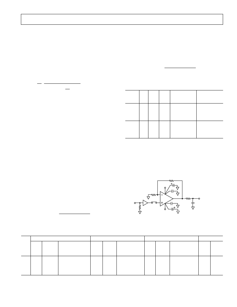
also recommended, as shown in Figure 24. Table IV contains
values of feedback and series resistors that result in the best
pulse response for a given load capacitance.
R
G
V
IN
SWITCH
R
F
R
T
50
V
OUT
(TO FET PROBE)
0.1μF
10μF
BUFFER
+V
S
0.1μF
10μF
–V
S
R
S(OUT)
C
L
Figure 24. Circuit for Driving a Capacitive Load
Table IV. Recommended Feedback and Series Resistors and Bandwidth vs. Capacitive Load and Gain
G = +1
G = +2
G = +3
G
r
+4
V
OUT
= 2 V p-p
–3 dB BW
(MHz)
V
OUT
= 2 V p-p
V
OUT
= 2 V p-p
–3 dB BW
(MHz)
C
L
(pF)
R
F
(
V
)
R
SOUT
(
V
)
R
F
(
V
)
R
SOUT
–3 dB BW
(
V
)
(MHz)
R
F
(
V
)
R
SOUT
(
V
)
R
F
(
V
)
R
SOUT
(
V
)
20
50
100
300
1 k
1 k
2k
2k
50
30
20
20
149
104
73
27
1 k
1 k
1 k
1 k
20
15
15
15
174
117
80
34
499
1 k
1 k
1 k
25
15
15
15
170
98
71
33
499
499
499
499
20
20
15
15
相关PDF资料 |
PDF描述 |
|---|---|
| AD8170AR-REEL | 250 MHz, 10 ns Switching Multiplexers w/Amplifier |
| AD8174-EB | 250 MHz, 10 ns Switching Multiplexers w/Amplifier |
| AD8174AN | 250 MHz, 10 ns Switching Multiplexers w/Amplifier |
| AD8174AR | 250 MHz, 10 ns Switching Multiplexers w/Amplifier |
| AD8174AR-REEL | VARISTOR 11VRMS 20MM RADIAL |
相关代理商/技术参数 |
参数描述 |
|---|---|
| AD8174 | 制造商:未知厂家 制造商全称:未知厂家 功能描述:AD8170/AD8174: 250 MHz. 10 ns Switching Multiplexers w/Amplifier Data Sheet (Rev. 0. 10/96) |
| AD8174AN | 制造商:Analog Devices 功能描述:Analog Multiplexer/Amp Single 4:1 14-Pin PDIP Tube 制造商:Rochester Electronics LLC 功能描述:PDIP 200MHZ 4:1 LOW POWER BUFFERED MUX - Bulk 制造商:Analog Devices 功能描述:IC MUX 4CH 250MHZ 8174 DIP14 |
| AD8174ANZ | 功能描述:IC MUX SW W/AMP 250MHZ 14-DIP RoHS:是 类别:集成电路 (IC) >> 接口 - 专用 系列:- 特色产品:NXP - I2C Interface 标准包装:1 系列:- 应用:2 通道 I²C 多路复用器 接口:I²C,SM 总线 电源电压:2.3 V ~ 5.5 V 封装/外壳:16-TSSOP(0.173",4.40mm 宽) 供应商设备封装:16-TSSOP 包装:剪切带 (CT) 安装类型:表面贴装 产品目录页面:825 (CN2011-ZH PDF) 其它名称:568-1854-1 |
| AD8174AR | 功能描述:IC MUX W/AMP BUFFERED 14-SOIC RoHS:否 类别:集成电路 (IC) >> 接口 - 专用 系列:- 特色产品:NXP - I2C Interface 标准包装:1 系列:- 应用:2 通道 I²C 多路复用器 接口:I²C,SM 总线 电源电压:2.3 V ~ 5.5 V 封装/外壳:16-TSSOP(0.173",4.40mm 宽) 供应商设备封装:16-TSSOP 包装:剪切带 (CT) 安装类型:表面贴装 产品目录页面:825 (CN2011-ZH PDF) 其它名称:568-1854-1 |
| AD8174AR-REEL | 制造商:Analog Devices 功能描述:Analog Multiplexer/Amp Single 4:1 14-Pin SOIC N T/R |
发布紧急采购,3分钟左右您将得到回复。