参数资料
| 型号: | AD8176ABPZ |
| 厂商: | Analog Devices Inc |
| 文件页数: | 30/40页 |
| 文件大小: | 0K |
| 描述: | IC VIDEO CROSSPOINT SWIT 676BGA |
| 标准包装: | 1 |
| 功能: | 视频交叉点开关 |
| 电路: | 3 x 16:9 |
| 电压电源: | 单/双电源 |
| 电压 - 电源,单路/双路(±): | 4.5 V ~ 5.5 V,±2.5V |
| 电流 - 电源: | 600mA |
| 工作温度: | -40°C ~ 85°C |
| 安装类型: | 表面贴装 |
| 封装/外壳: | 676-BGA |
| 供应商设备封装: | 676-BGA(27x27) |
| 包装: | 管件 |
第1页第2页第3页第4页第5页第6页第7页第8页第9页第10页第11页第12页第13页第14页第15页第16页第17页第18页第19页第20页第21页第22页第23页第24页第25页第26页第27页第28页第29页当前第30页第31页第32页第33页第34页第35页第36页第37页第38页第39页第40页
AD8176
Rev. 0 | Page 36 of 40
PCB Termination Layout
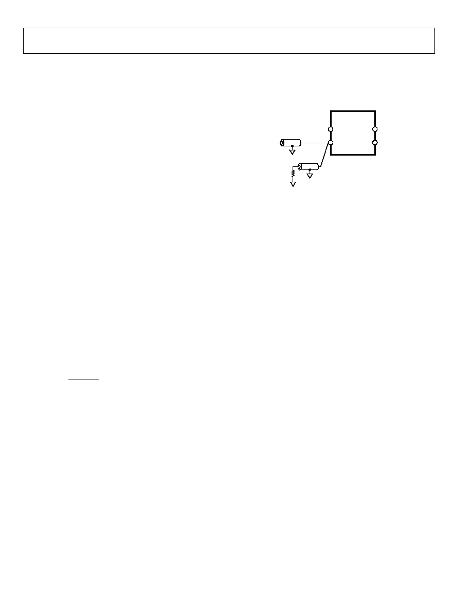
If multiple AD8176s are to be driven in parallel, a fly-by input
termination scheme is very useful, but the distance from each
AD8176 input to the driven input transmission line is a stub
that should be minimized in length and parasitics using the
discussed guidelines.
As frequencies of operation increase, the importance of proper
transmission line signal routing becomes more important. The
bandwidth of the AD8176 is large enough that using high
impedance routing does not provide a flat in-band frequency
response for practical signal trace lengths. It is necessary for the
user to choose a characteristic impedance suitable for the applica-
tion and properly terminate the input and output signals of the
AD8176. Traditionally, video applications have used 75 Ω
single-ended environments. RF applications are generally 50 Ω
single-ended (and board manufacturers have the most experience
with this application). CAT- cabling is usually driven as
differential pairs of 100 Ω differential impedance.
AD8176
OPn
ONn
IPn
INn
50
0
65
96
-0
26
For flexibility, the AD8176 does not contain on-chip termina-
tion resistors. This flexibility in application comes with some
board layout challenges. The distance between the termination
of the input transmission line and the AD8176 die is a high
impedance stub, and causes reflections of the input signal. With
some simplification, it can be shown that these reflections cause
peaking of the input at regular intervals in frequency, dependent
on the propagation speed (VP) of the signal in the chosen board
material and the distance (d) between the termination resistor
and the AD8176. If the distance is great enough, these peaks
can occur in-band. In fact, practical experience shows that these
peaks are not high-Q, and should be pushed out to three or four
times the desired bandwidth in order to not have an effect on
the signal. For a board designer using FR4 (VP = 144 × 106 m/s),
this means the AD8176 should be no more than 1.5 cm after the
termination resistors, and preferably should be placed even
closer. The BGA substrate routing inside the AD8176 is approxi-
mately 1 cm in length and adds to the stub length, so 1.5 cm
PCB routing equates to d = 2.5 × 10⁻² m in the calculations.
Figure 52. Fly-By Input Termination (Grounds for the two transmission lines
shown must be tied together close to the INn pin)
(
)
d
V
n
f
P
PEAK
4
1
2 +
=
(12)
When driving the AD8176 single-endedly, the undriven input is
often terminated with a resistance to balance the input stage. It
can be seen that by terminating the undriven input with a
resistor of one-half the characteristic impedance, the input stage
will be perfectly balanced (25 Ω, for example, to balance the two
parallel 50 Ω terminations on the driven input). However, due
to the feedback in the input receiver, there is high speed signal
current leaving the undriven input. To terminate this high
speed signal, proper transmission line techniques should be
used. One solution is to adjust the trace width to create a
transmission line of half the characteristic impedance and
terminate the far end with this resistance (25 Ω in a 50 Ω
system). This is not often practical as trace widths become large.
In most cases, the best practical solution is to place the half-
characteristic impedance resistor as close as possible (preferably
less than 1.5 cm away) and to reduce the parasitics of the stub
(by removing the ground plane under the stub, for example). In
either case, the designer must decide if the layout complexity
created by a balanced, terminated solution is preferable to
simply grounding the undriven input at the ball with no trace.
where n = {0, 1, 2, 3, …}.
While the examples discussed so far are for input termination,
the theory is similar for output back-termination. Taking the
AD8176 as an ideal voltage source, any distance of routing
between the AD8176 and a back-termination resistor will be an
impedance mismatch that potentially creates reflections. For
this reason, back-termination resistors should also be placed
close to the AD8176. In practice, because back-termination
resistors are series elements, they can be placed close to the
AD8176 outputs.
In some cases, it is difficult to place the termination close to the
AD8176 due to space constraints, differential routing, and large
resistor footprints. A preferable solution in this case is to
maintain a controlled transmission line past the AD8176 inputs
and terminate the end of the line. This is known as fly-by
termination. The input impedance of the AD8176 is large
enough and stub length inside the package is small enough that
this works well in practice. Implementation of fly-by input
termination often includes bringing the signal in on one routing
layer, then passing through a filled-via under the AD8176 input
ball, then back out to termination on another signal layer. In
this case, care must be taken to tie the reference ground planes
together near the signal via if the signal layers are referenced to
different ground planes.
Finally, the AD8176 pinout allows the user to bring the outputs
out as surface traces to the back-termination resistors. The
designer can avoid creating stubs and reflections by keeping the
AD8176 output signal path on the surface of the board. A stub
is created when a top-to-bottom via connection is made on the
output signal path that is perpendicular to the signal flow.
相关PDF资料 |
PDF描述 |
|---|---|
| AD8177ABPZ | IC VIDEO CROSSPOINT SWIT 676BGA |
| AD8178ABPZ | IC VIDEO CROSSPOINT SWIT 676BGA |
| AD8182ANZ | IC MULTIPLEXER DUAL 2X1 14DIP |
| AD8184AR | IC VIDEO MULTIPLEXER 4X1 14SOIC |
| AD8185ARUZ | IC MULTIPLEXER TRPL 2X1 24TSSOP |
相关代理商/技术参数 |
参数描述 |
|---|---|
| AD8176-EVAL | 制造商:AD 制造商全称:Analog Devices 功能描述:475 MHz, Triple 16 】 9 Video Crosspoint Switch |
| AD8177 | 制造商:AD 制造商全称:Analog Devices 功能描述:500 MHz, Triple 16 】 5 Video Crosspoint Switch |
| AD8177ABPZ | 功能描述:IC VIDEO CROSSPOINT SWIT 676BGA RoHS:是 类别:集成电路 (IC) >> 接口 - 模拟开关,多路复用器,多路分解器 系列:- 其它有关文件:STG4159 View All Specifications 标准包装:5,000 系列:- 功能:开关 电路:1 x SPDT 导通状态电阻:300 毫欧 电压电源:双电源 电压 - 电源,单路/双路(±):±1.65 V ~ 4.8 V 电流 - 电源:50nA 工作温度:-40°C ~ 85°C 安装类型:表面贴装 封装/外壳:7-WFBGA,FCBGA 供应商设备封装:7-覆晶 包装:带卷 (TR) |
| AD8177-EVALZ | 制造商:AD 制造商全称:Analog Devices 功能描述:500 MHz, Triple 16 】 5 Video Crosspoint Switch |
| AD8178 | 制造商:AD 制造商全称:Analog Devices 功能描述:450 MHz, Triple 16 】 5 Video Crosspoint Switch |
发布紧急采购,3分钟左右您将得到回复。