- 您现在的位置:买卖IC网 > PDF目录373939 > AD8178 (Analog Devices, Inc.) 450 MHz, Triple 16 】 5 Video Crosspoint Switch PDF资料下载
参数资料
| 型号: | AD8178 |
| 厂商: | Analog Devices, Inc. |
| 英文描述: | 450 MHz, Triple 16 】 5 Video Crosspoint Switch |
| 中文描述: | 450兆赫,三16】5视频交叉点开关 |
| 文件页数: | 7/40页 |
| 文件大小: | 545K |
| 代理商: | AD8178 |
第1页第2页第3页第4页第5页第6页当前第7页第8页第9页第10页第11页第12页第13页第14页第15页第16页第17页第18页第19页第20页第21页第22页第23页第24页第25页第26页第27页第28页第29页第30页第31页第32页第33页第34页第35页第36页第37页第38页第39页第40页
AD8178
ABSOLUTE MAXIMUM RATINGS
Rev. 0 | Page 7 of 40
Table 12.
Parameter
Analog Supply Voltage (V
POS
– V
NEG
)
Digital Supply Voltage (V
DD
– D
GND
)
Ground Potential Difference
(V
NEG
– D
GND
)
Maximum Potential Difference
(V
DD
– V
NEG
)
Common-Mode Analog Input Voltage
Rating
6 V
6 V
+0.5 V to –2.5 V
8 V
(V
NEG
– 0.5 V) to
(V
POS
+ 0.5 V)
±2 V
V
DD
(V
POS
– 1 V) to (V
NEG
+ 1 V)
Differential Analog Input Voltage
Digital Input Voltage
Output Voltage
(Disabled Analog Output)
Output Short-Circuit Duration
Storage Temperature Range
Operating Temperature Range
Lead Temperature
(Soldering, 10 sec)
Junction Temperature
Momentary
65°C to +125°C
40°C to +85°C
300°C
150°C
Stresses above those listed under Absolute Maximum Ratings
may cause permanent damage to the device. This is a stress
rating only; functional operation of the device at these or any
other conditions above those indicated in the operational
section of this specification is not implied. Exposure to absolute
maximum rating conditions for extended periods may affect
device reliability.
THERMAL RESISTANCE
θ
JA
is specified for the worst-case conditions, that is, a device
soldered in a circuit board for surface-mount packages.
Table 13. Thermal Resistance
Package Type
PBGA
θ
JA
15
Unit
°C/W
POWER DISSIPATION
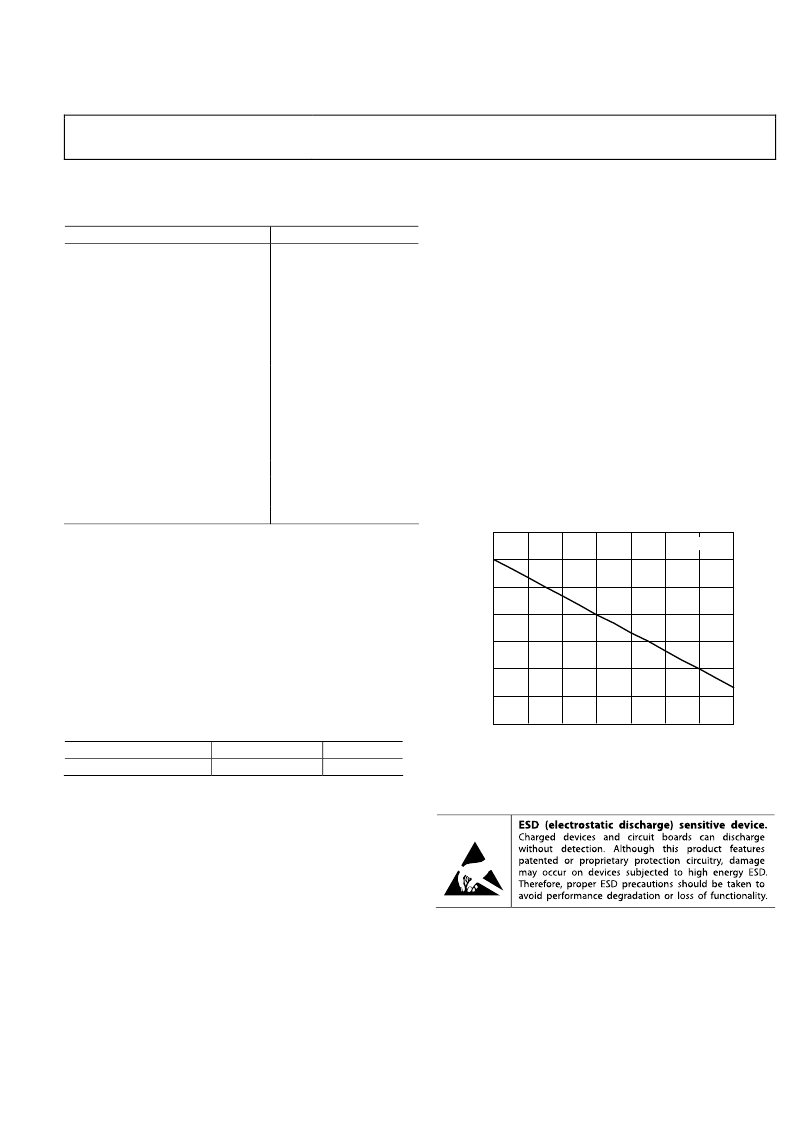
The AD8178 is operated with ±2.5 V or +5 V supplies and can
drive loads down to 100 Ω, resulting in a large range of possible
power dissipations. For this reason, extra care must be taken
when derating the operating conditions based on ambient
temperature.
Packaged in a 676-lead BGA, the AD8178 junction-to-ambient
thermal impedance (
θ
JA
) is 15°C/W. For long-term reliability,
the maximum allowed junction temperature of the die should
not exceed 150°C. Temporarily exceeding this limit may cause
a shift in parametric performance due to a change in stresses
exerted on the die by the package. Exceeding a junction
temperature of 175°C for an extended period can result in
device failure. The curve in Figure 4 shows the range of allowed
internal die power dissipations that meet these conditions over
the 40°C to +85°C ambient temperature range. When using
Table 13, do not include external load power in the maximum
power calculation, but do include load current dropped on the
die output transistors.
0
AMBIENT TEMPERATURE (°C)
M
3
4
5
6
7
8
9
10
15
25
35
45
55
65
75
85
T
J
= 150°C
Figure 4. Maximum Die Power Dissipation vs. Ambient Temperature
ESD CAUTION
相关PDF资料 |
PDF描述 |
|---|---|
| AD8178ABPZ1 | 450 MHz, Triple 16 】 5 Video Crosspoint Switch |
| AD8178-EVALZ1 | 450 MHz, Triple 16 】 5 Video Crosspoint Switch |
| AD817 | High Speed, Low Power Wide Supply Range Amplifier(高速,低功耗,宽电源范围放大器) |
| AD8180-EB | 750 MHz, 3.8 mA 10 ns Switching Multiplexers |
| AD8180AN | 750 MHz, 3.8 mA 10 ns Switching Multiplexers |
相关代理商/技术参数 |
参数描述 |
|---|---|
| AD8178ABPZ | 功能描述:IC VIDEO CROSSPOINT SWIT 676BGA RoHS:是 类别:集成电路 (IC) >> 接口 - 模拟开关,多路复用器,多路分解器 系列:- 其它有关文件:STG4159 View All Specifications 标准包装:5,000 系列:- 功能:开关 电路:1 x SPDT 导通状态电阻:300 毫欧 电压电源:双电源 电压 - 电源,单路/双路(±):±1.65 V ~ 4.8 V 电流 - 电源:50nA 工作温度:-40°C ~ 85°C 安装类型:表面贴装 封装/外壳:7-WFBGA,FCBGA 供应商设备封装:7-覆晶 包装:带卷 (TR) |
| AD8178ABPZ1 | 制造商:AD 制造商全称:Analog Devices 功能描述:450 MHz, Triple 16 】 5 Video Crosspoint Switch |
| AD8178-EVALZ1 | 制造商:AD 制造商全称:Analog Devices 功能描述:450 MHz, Triple 16 】 5 Video Crosspoint Switch |
| AD817AN | 功能描述:IC OPAMP HS LP 8-DIP RoHS:否 类别:集成电路 (IC) >> 线性 - 放大器 - 视频放大器和频缓冲器 系列:- 产品培训模块:Lead (SnPb) Finish for COTS Obsolescence Mitigation Program 标准包装:50 系列:- 应用:TFT-LCD 面板:VCOM 驱动器 输出类型:满摆幅 电路数:1 -3db带宽:35MHz 转换速率:40 V/µs 电流 - 电源:3.7mA 电流 - 输出 / 通道:1.3A 电压 - 电源,单路/双路(±):9 V ~ 20 V,±4.5 V ~ 10 V 安装类型:表面贴装 封装/外壳:8-TSSOP,8-MSOP(0.118",3.00mm 宽)裸露焊盘 供应商设备封装:8-uMax-EP 包装:管件 |
| AD817AN | 制造商:Analog Devices 功能描述:SEMICONDUCTORSLINEAR |
发布紧急采购,3分钟左右您将得到回复。