- 您现在的位置:买卖IC网 > PDF目录373939 > AD817 (Analog Devices, Inc.) High Speed, Low Power Wide Supply Range Amplifier(高速,低功耗,宽电源范围放大器) PDF资料下载
参数资料
| 型号: | AD817 |
| 厂商: | Analog Devices, Inc. |
| 英文描述: | High Speed, Low Power Wide Supply Range Amplifier(高速,低功耗,宽电源范围放大器) |
| 中文描述: | 高速,低功耗,宽电源电压范围放大器(高速,低功耗,宽电源范围放大器) |
| 文件页数: | 11/12页 |
| 文件大小: | 331K |
| 代理商: | AD817 |
AD817
REV. B
–11–
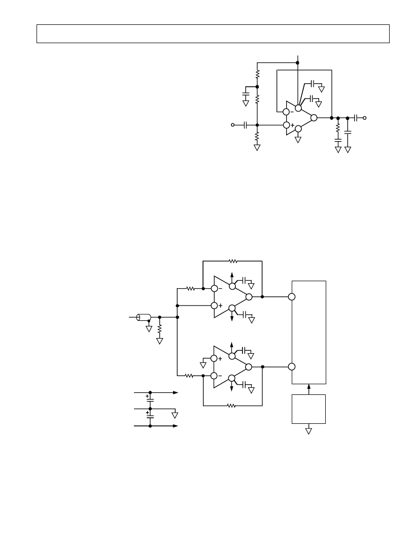
A HIGH PE RFORMANCE ADC INPUT BUFFE R
High performance analog to digital converters (ADCs) require
input buffers with correspondingly high bandwidths and very
low levels of distortion. T ypical requirements include distortion
levels of –60 dB to –70 dB for a 1 volt p-p signal and band-
widths of 10 MHz or more. In addition, an ADC buffer may
need to drive very large capacitive loads.
T he circuit of Figure 36 is useful for driving high speed convert-
ers such as the differential input of the AD733, 10-bit ADC.
T his circuit may be used with other converters with only minor
modifications. Using the AD817 provides the user with the op-
tion of either operating the buffer in differential mode or from a
single +5 volt supply. Operating from a +5 volt power supply
helps to avoid overdriving the ADC—a common problem with
buffers operating at higher supply voltages.
SINGLE SUPPLY OPE RAT ION
Another exciting feature of the AD817 is its ability to perform
well in a single supply configuration. T he AD817 is ideally
suited for applications that require low power dissipation and
high output current and those which need to drive large capaci-
tive loads, such as high speed buffering and instrumentation.
Referring to Figure 37, careful consideration should be given to
the proper selection of component values. T he choices for this
particular circuit are: R1+ R3//R2 combine with C1 to form a
low frequency corner of approximately 300 Hz.
R2
10k
C3
0.1
μ
F
R1
9k
R3
1k
C2
0.1
μ
F
C1
0.1
μ
F
C
200pF
R
L
150
SELECT C1, R1, R2 & R3
FOR DESIRED LOW
FREQUENCY CORNER.
(R2 = R1 + R3)
C
OUT
+V
S
V
OUT
V
IN
AD817
7
6
3
2
4
0.01
μ
F
3.3
μ
F
Figure 37. Single Supply Amplifier Configuration
Combining R3 with C2 forms a low-pass filter with a corner
frequency of 1.5 kHz. T his is needed to maintain amplifier
PSRR, since the supply is connected to V
IN
through the input
divider. T he values for R
L
and C
L
were chosen to demonstrate
the AD817’s exceptional output drive capability. In this con-
figuration, the output is centered around 2.5 V. In order to
eliminate the static dc current associated with this level, C3 was
inserted in series with R
L
.
52.5
0.1
μ
F
1k
0.1
μ
F
–V
S
1k
1k
1k
AD773
10-BIT
18MHz
ADC
V
INA
V
INB
ADREF43
VOLTAGE
REFERENCE
+2.5V
50
COAX
CABLE
V
IN
500mVp-p
MAX
+V
S
AD817
7
6
3
2
4
26
27
0.1
μ
F
0.1
μ
F
–V
S
+V
S
AD817
7
6
3
2
4
+5V
COMMON
–5V
100
μ
F
25V
100
μ
F
25V
+V
S
–V
S
Figure 36. A Differential Input Buffer for High Bandwidth ADCs
相关PDF资料 |
PDF描述 |
|---|---|
| AD8180-EB | 750 MHz, 3.8 mA 10 ns Switching Multiplexers |
| AD8180AN | 750 MHz, 3.8 mA 10 ns Switching Multiplexers |
| AD8180AR | 750 MHz, 3.8 mA 10 ns Switching Multiplexers |
| AD8180AR-REEL | 750 MHz, 3.8 mA 10 ns Switching Multiplexers |
| AD8180AR-REEL7 | 750 MHz, 3.8 mA 10 ns Switching Multiplexers |
相关代理商/技术参数 |
参数描述 |
|---|---|
| AD8170 | 制造商:AD 制造商全称:Analog Devices 功能描述:250 MHz, 10 ns Switching Multiplexers w/Amplifier |
| AD8170AN | 制造商:Analog Devices 功能描述:Analog Multiplexer Single 2:1 8-Pin PDIP Tube 制造商:Analog Devices 功能描述:IC MUX 2CH 250MHZ 8170 DIP8 |
| AD8170ANZ | 功能描述:IC MUX SWITCHING W/AMP 2:1 8DIP RoHS:是 类别:集成电路 (IC) >> 接口 - 专用 系列:- 特色产品:NXP - I2C Interface 标准包装:1 系列:- 应用:2 通道 I²C 多路复用器 接口:I²C,SM 总线 电源电压:2.3 V ~ 5.5 V 封装/外壳:16-TSSOP(0.173",4.40mm 宽) 供应商设备封装:16-TSSOP 包装:剪切带 (CT) 安装类型:表面贴装 产品目录页面:825 (CN2011-ZH PDF) 其它名称:568-1854-1 |
| AD8170AR | 功能描述:IC MUX W/AMP BUFFERED 8-SOIC RoHS:否 类别:集成电路 (IC) >> 接口 - 专用 系列:- 特色产品:NXP - I2C Interface 标准包装:1 系列:- 应用:2 通道 I²C 多路复用器 接口:I²C,SM 总线 电源电压:2.3 V ~ 5.5 V 封装/外壳:16-TSSOP(0.173",4.40mm 宽) 供应商设备封装:16-TSSOP 包装:剪切带 (CT) 安装类型:表面贴装 产品目录页面:825 (CN2011-ZH PDF) 其它名称:568-1854-1 |
| AD8170AR-REEL | 制造商:Analog Devices 功能描述:Analog Multiplexer Single 2:1 8-Pin SOIC N T/R 制造商:Rochester Electronics LLC 功能描述:SOIC 2:1 BUFFERED MULTIPLEXER - Tape and Reel |
发布紧急采购,3分钟左右您将得到回复。