- 您现在的位置:买卖IC网 > PDF目录11233 > AD8180ARZ-R7 (Analog Devices Inc)IC MULTIPLEXER 2X1 8SOIC PDF资料下载
参数资料
| 型号: | AD8180ARZ-R7 |
| 厂商: | Analog Devices Inc |
| 文件页数: | 10/12页 |
| 文件大小: | 0K |
| 描述: | IC MULTIPLEXER 2X1 8SOIC |
| 标准包装: | 750 |
| 功能: | 多路复用器 |
| 电路: | 1 x 2:1 |
| 电压电源: | 双电源 |
| 电压 - 电源,单路/双路(±): | ±4 V ~ 6 V |
| 工作温度: | -40°C ~ 85°C |
| 安装类型: | 表面贴装 |
| 封装/外壳: | 8-SOIC(0.154",3.90mm 宽) |
| 供应商设备封装: | 8-SOIC |
| 包装: | 带卷 (TR) |
AD8180/AD8182
–7–
REV. B
for RL > 10 k
. For heavier loads, the dc gain is approximately
that of the voltage divider formed by the output impedance of
the mux (typically 27
) and R
L.
High speed disable clamp circuits at the bases of Q5–Q8 (not
shown) allow the buffers to turn off quickly and cleanly without
dissipating much power once off. Moreover, these clamps shunt
displacement currents flowing through the junction capacitances
of Q1–Q4 away from the bases of Q5–Q8 and to ac ground
through low impedances. The two-pole high pass frequency
response of the T switch formed by these clamps is a significant
improvement over the one-pole high pass response of a simple
series CMOS switch. As a result, board and package parasitics,
especially stray capacitance between inputs and outputs may
limit the achievable crosstalk and off isolation.
LAYOUT CONSIDERATIONS:
Realizing the high speed performance attainable with the
AD8180 and AD8182 requires careful attention to board layout
and component selection. Proper RF design techniques and low
parasitic component selection are mandatory.
Wire wrap boards, prototype boards, and sockets are not recom-
mended because of their high parasitic inductance and capaci-
tance. Instead, surface-mount components should be soldered
directly to a printed circuit board (PCB). The PCB should have
a ground plane covering all unused portions of the component
side of the board to provide a low impedance ground path. The
ground plane should be removed from the area near input and
output pins to reduce stray capacitance.
Chip capacitors should be used for supply bypassing. One end
of the capacitor should be connected to the ground plane and
the other within 1/4 inch of each power pin. An additional large
(4.7
F–10 F) tantalum capacitor should be connected in
parallel with each of the smaller capacitors for low impedance
supply bypassing over a broad range of frequencies.
Signal traces should be as short as possible. Stripline or micros-
trip techniques should be used for long signal traces (longer
than about 1 inch). These should be designed with a character-
istic impedance of 50
or 75 and be properly terminated at
the end using surface mount components.
Careful layout is imperative to minimize crosstalk. Guards
(ground or supply traces) must be run between all signal traces
to limit direct capacitive coupling. Input and output signal lines
should fan out away from the mux as much as possible. If mul-
tiple signal layers are available, a buried stripline structure hav-
ing ground plane above, below, and between signal traces will
have the best crosstalk performance.
Return currents flowing through termination resistors can also
increase crosstalk if these currents flow in sections of the finite-
impedance ground circuit that is shared between more than one
input or output. Minimizing the inductance and resistance of the
ground plane can reduce this effect, but further care should be
taken in positioning the terminations. Terminating cables directly
at the connectors will minimize the return current flowing on the
board, but the signal trace between the connector and the mux will
look like an open stub and will degrade the frequency response.
Moving the termination resistors close to the input pins will im-
prove the frequency response, but the terminations from neigh-
boring inputs should not have a common ground return.
THEORY OF OPERATION
The AD8180 and AD8182 video multiplexers are designed for
fast-switching (10 ns) and wide bandwidth (> 750 MHz). This
performance is attained with low power dissipation (3.8 mA per
active channel) through the use of proprietary circuit techniques
and a dielectrically-isolated complementary bipolar process.
These devices have a fast disable function that allows the out-
puts of several muxes to be wired in parallel to form a larger mux
with little degradation in switching time. The low disabled output
capacitance (1.7 pF) of these muxes helps to preserve the system
bandwidth in larger matrices. Unlike earlier CMOS switches,
the switched open-loop buffer architecture of the AD8180 and
AD8182 provides a unidirectional signal path with minimal switch-
ing glitches and constant, low input capacitance. Since the input
impedance of these muxes is nearly independent of the load imped-
ance and the state of the mux, the frequency response of the ON
channels in a large switch matrix is not affected by fanout.
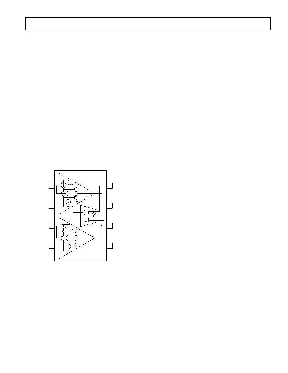
Figure 22 shows a block diagram and simplified schematic of the
AD8180, which contains two switched buffers (S0 and S1) that
share a common output. The decoder logic translates TTL-
compatible logic inputs (SELECT and
ENABLE) to internal,
differential ECL levels for fast, low-glitch switching. The SELECT
input determines which of the two buffers is enabled, unless the
ENABLE input is HIGH, in which case both buffers are disabled
and the output is switched to a high impedance state.
Q5
Q7
Q3
Q1
S0
I1
I3
Q6
Q8
Q4
Q2
S1
I2
I4
DECODER
AD8180
1
2
3
4
IN0
GND
IN1
+VS
8
7
6
5
–VS
OUT
ENABLE
SELECT
Figure 22. Block Diagram and Simplified Schematic of the
AD8180 Multiplexer
Each open-loop buffer is implemented as a complementary
emitter follower that provides high input impedance, symmetric
slew rate and load drive, and high output-to-input isolation due to
its
β2 current gain. The selected buffer is biased ON by fast
switched current sources that allow the buffer to turn on quickly.
Dedicated flatness circuits, combined with the open-loop architec-
ture of the AD8180 and AD8182, keep peaking low (typically
< 1 dB) when driving high capacitive loads, without the need for
external series resistors at the input or output. If better flatness
response is desired, an input series resistance (RS) may be used
(refer to Figure 20), although this will increase crosstalk. The dc
gain of the AD8180 and AD8182 is almost independent of load
相关PDF资料 |
PDF描述 |
|---|---|
| ADG411BRU-REEL7 | IC SWITCH QUAD SPST 16TSSOP |
| VE-2NZ-IV-F4 | CONVERTER MOD DC/DC 2V 60W |
| VI-2ND-IY-S | CONVERTER MOD DC/DC 85V 50W |
| VE-2NY-IV-F4 | CONVERTER MOD DC/DC 3.3V 99W |
| RDER72J104K8K1C11B | CAP CER 0.1UF 630V 10% RADIAL |
相关代理商/技术参数 |
参数描述 |
|---|---|
| AD8180ARZ-RL | 功能描述:IC MULTIPLEXER 2X1 8SOIC RoHS:是 类别:集成电路 (IC) >> 接口 - 模拟开关,多路复用器,多路分解器 系列:- 标准包装:1,000 系列:- 功能:多路复用器 电路:1 x 4:1 导通状态电阻:- 电压电源:双电源 电压 - 电源,单路/双路(±):±5V 电流 - 电源:7mA 工作温度:-40°C ~ 85°C 安装类型:表面贴装 封装/外壳:16-SOIC(0.154",3.90mm 宽) 供应商设备封装:16-SOIC 包装:带卷 (TR) |
| AD8180-EB | 制造商:Analog Devices 功能描述:AD8180 EVALUATION BOARD - Bulk |
| AD8182 | 制造商:AD 制造商全称:Analog Devices 功能描述:750 MHz, 3.8 mA 10 ns Switching Multiplexers |
| AD8182AN | 制造商:Analog Devices 功能描述:Analog Multiplexer Dual 2:1 14-Pin PDIP 制造商:Rochester Electronics LLC 功能描述:DUAL 2:1 800MHZ,3.5MA,10NS SWITCHING MUX - Bulk 制造商:Analog Devices 功能描述:SEMICONDUCTOR ((NS)) 制造商:Analog Devices 功能描述:750 MHz, 3.8 mA 10 ns Switching Multiplexers 制造商:Analog Devices Inc. 功能描述:750 MHz, 3.8 mA 10 ns Switching Multiplexers |
| AD8182ANZ | 功能描述:IC MULTIPLEXER DUAL 2X1 14DIP RoHS:是 类别:集成电路 (IC) >> 接口 - 模拟开关,多路复用器,多路分解器 系列:- 其它有关文件:STG4159 View All Specifications 标准包装:5,000 系列:- 功能:开关 电路:1 x SPDT 导通状态电阻:300 毫欧 电压电源:双电源 电压 - 电源,单路/双路(±):±1.65 V ~ 4.8 V 电流 - 电源:50nA 工作温度:-40°C ~ 85°C 安装类型:表面贴装 封装/外壳:7-WFBGA,FCBGA 供应商设备封装:7-覆晶 包装:带卷 (TR) |
发布紧急采购,3分钟左右您将得到回复。