- 您现在的位置:买卖IC网 > PDF目录11235 > AD8188ARUZ-R7 (Analog Devices Inc)IC MULTIPLEXER TRPL 2X1 24TSSOP PDF资料下载
参数资料
| 型号: | AD8188ARUZ-R7 |
| 厂商: | Analog Devices Inc |
| 文件页数: | 11/24页 |
| 文件大小: | 0K |
| 描述: | IC MULTIPLEXER TRPL 2X1 24TSSOP |
| 标准包装: | 1,000 |
| 功能: | 多路复用器 |
| 电路: | 3 x 2:1 |
| 电压电源: | 单电源 |
| 电压 - 电源,单路/双路(±): | 3.5 V ~ 5.5 V |
| 工作温度: | -40°C ~ 85°C |
| 安装类型: | 表面贴装 |
| 封装/外壳: | 24-TSSOP(0.173",4.40mm 宽) |
| 供应商设备封装: | 24-TSSOP |
| 包装: | 带卷 (TR) |
AD8188/AD8189
Rev. 0 | Page 19 of 24
These two techniques can also be combined. Typically, crosstalk
between the RGB signals from the same source is less objectionable
than crosstalk between two different sources. The former can
cause a color or luminance shift, but spatially, everything is
coherent. However, the crosstalk signals from two uncorrelated
sources can create ghost images that are far more objectionable.
A technique for minimizing crosstalk between two different
sources is to create two separate VMID circuits. Then, the inputs
from each source can be connected to their own VMID node,
minimizing crosstalk between sources.
AD8189
When using the gain-of-two AD8189 in a simple ac-coupled
application, there is a dynamic range limitation at the output
caused by its higher gain. At the output, the gain-of-two
produces a signal swing of 1.4 V, but the ac-coupling doubles
this required amount to 2.8 V. The AD8189 outputs can only
swing from 1.4 V to 3.6 V on a 5 V supply, so there are only
2.2 V of dynamic signal swing available at the output.
A standard means for reducing the dynamic range requirements
of an ac-coupled video signal is to use a dc restore. This circuit
works to limit the dynamic range requirements by clamping the
black level of the video signal to a fixed level at the input to the
amplifier. This prevents the video content of the signal from
varying the black level, as happens in a simple ac-coupled circuit.
DC RESTORE
After ac-coupling a video signal, it is necessary to use a dc
restore to establish where the black level is. Usually, this appears
at the end of a video signal chain. This dc restore circuit needs
to have the required accuracy for the system. It compensates for
all the offsets of the preceding stages. Therefore, if a dc restore
circuit is to be used only for dynamic range limiting, it does not
require great dc accuracy.
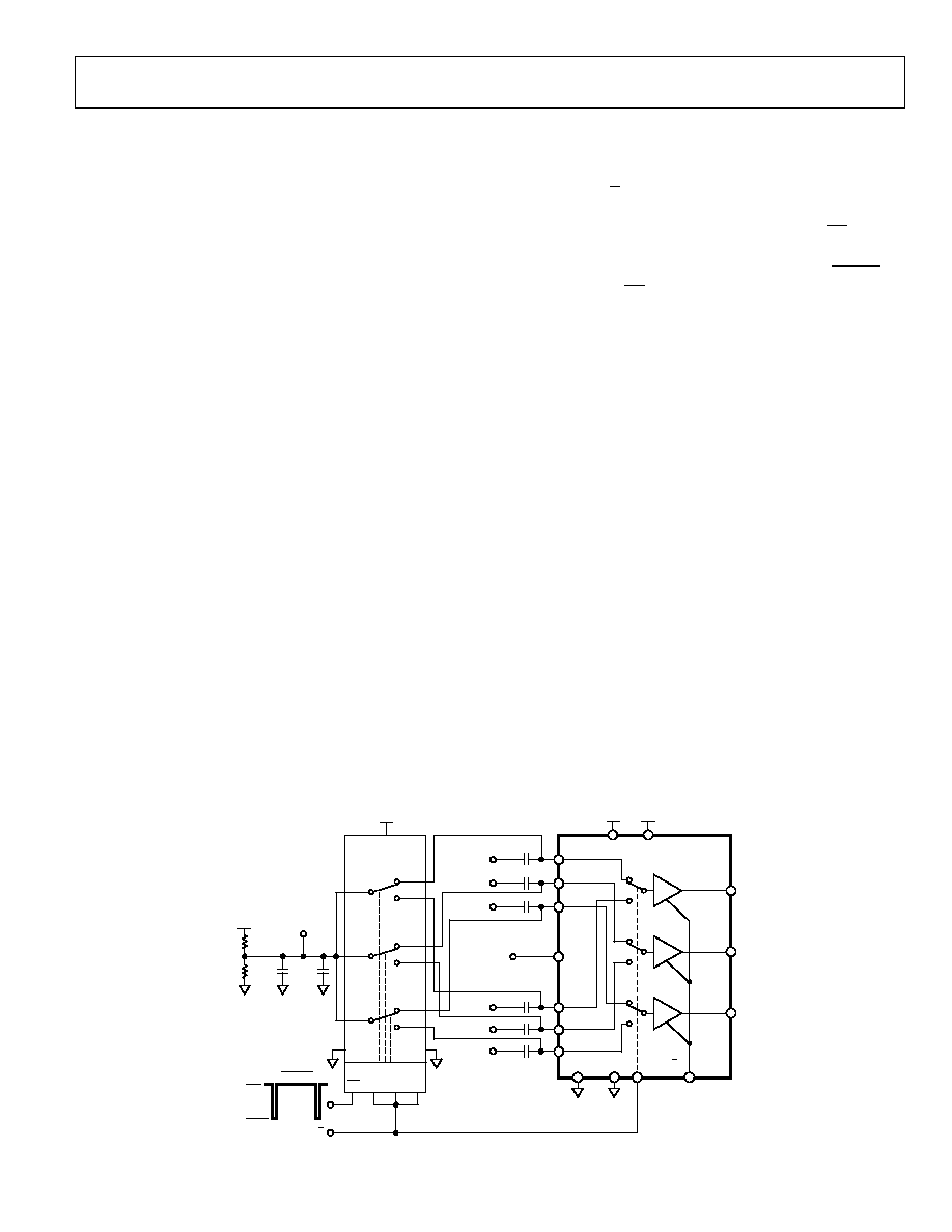
A dc restore circuit using the AD8189 is shown in Figure 56.
Two separate sources of RGB video are ac-coupled to the 0.1 μF
input capacitors of the AD8189. The input points of the
AD8189 are switched to a 1.5 V reference by the ADG786,
which works in the following manner:
The SEL A/B signal selects the A or B input to the AD8189. It
also selects the switch positions in the ADG786 such that the
same selected inputs are connected to VREF when EN is low.
During the horizontal interval, all of the RGB input signals are
at a flat black level. A logic signal that is low during HSYNC is
applied to the EN of the ADG786. This closes the switches and
clamps the black level to 1.5 V. At all other times, the switches
are off and the node at the inputs to the AD8189 floats.
There are two considerations for sizing the input coupling
capacitors. One is the time constant during the H-pulse
clamping. The other is the droop associated with the capacitor
discharge due to the input bias current of the AD8189. For the
former, it is better to have a small capacitor, but for the latter, a
larger capacitor is better.
The on resistance of the ADG786 and the coupling capacitor
form the time constant of the input clamp. The ADG786 on
resistance is 5 Ω maximum. With a 0.1 μF capacitor, a time
constant of 0.5 μs is created. Thus, a sync pulse of greater than
2.5 μs causes less than 1% error. This is not critical because the
black level from successive lines is very close and the voltage
changes little from line to line.
A rough approximation of the horizontal line time for a graphics
system is 30 μs. This varies depending on the resolution and the
vertical rate. The coupling capacitor needs to hold the voltage
relatively constant during this time, while the input bias current
of the AD8189 discharges it.
The change in voltage is IB times the line time divided by the
capacitance. With an IB of 2.5 μA, a line time of 30 μs, and a
0.1 μF coupling capacitor, the amount of droop is 0.75 mV. This
is roughly 0.1% of the full video amplitude and is not observable
in the video display.
VEE
DGND
RED
GRN
BLU
REDA
GRNA
BLUA
IN2B
IN1B
IN0B
IN0A
IN1A
IN2A
VREF
BLUB
GRNB
REDB
DVCC
SEL A/B
OE
×2
OUT0
OUT1
OUT2
VCC
×2
AD8189
3V TO 5V 5V
0.1F
S1A
S1B
S2A
S2B
S3A
S3B
VDD
5V
D1
D2
D3
GND
VSS
EN A0 A1 A2
+
5V
1.5k
3.48k
1.5V
VREF
10F
0.1F
ADG786
LOGIC
SEL A/B
HSYNC
2.4V MIN
0.8V MIN
0
62
39
-05
6
Figure 56. AD8189 AC-Coupled with DC Restore
相关PDF资料 |
PDF描述 |
|---|---|
| VE-J6X-IX-F1 | CONVERTER MOD DC/DC 5.2V 75W |
| ADG729BRU-REEL | IC MUX/DEMUX DUAL 4X1 16TSSOP |
| VE-J6W-IX-F1 | CONVERTER MOD DC/DC 5.5V 75W |
| ADG728BRU-REEL | IC MUX/DEMUX 8X1 16TSSOP |
| VE-J6V-IX-F2 | CONVERTER MOD DC/DC 5.8V 75W |
相关代理商/技术参数 |
参数描述 |
|---|---|
| AD8188ARUZ-RL | 功能描述:IC MULTIPLEXER TRPL 2:1 24TSSOP RoHS:是 类别:集成电路 (IC) >> 接口 - 模拟开关,多路复用器,多路分解器 系列:- 标准包装:1,000 系列:- 功能:多路复用器 电路:1 x 4:1 导通状态电阻:- 电压电源:双电源 电压 - 电源,单路/双路(±):±5V 电流 - 电源:7mA 工作温度:-40°C ~ 85°C 安装类型:表面贴装 封装/外壳:16-SOIC(0.154",3.90mm 宽) 供应商设备封装:16-SOIC 包装:带卷 (TR) |
| AD8188Z-EVALZ | 制造商:AD 制造商全称:Analog Devices 功能描述:350 MHz Single-Supply (5 V) Triple 2:1 Multiplexers |
| AD8189 | 制造商:AD 制造商全称:Analog Devices 功能描述:350 MHz Single-Supply (5 V) Triple 2:1 Multiplexers |
| AD8189ARUZ | 功能描述:IC MULTIPLEXER TRPL 2X1 24TSSOP RoHS:是 类别:集成电路 (IC) >> 接口 - 模拟开关,多路复用器,多路分解器 系列:- 其它有关文件:STG4159 View All Specifications 标准包装:5,000 系列:- 功能:开关 电路:1 x SPDT 导通状态电阻:300 毫欧 电压电源:双电源 电压 - 电源,单路/双路(±):±1.65 V ~ 4.8 V 电流 - 电源:50nA 工作温度:-40°C ~ 85°C 安装类型:表面贴装 封装/外壳:7-WFBGA,FCBGA 供应商设备封装:7-覆晶 包装:带卷 (TR) |
| AD8189ARUZ-R7 | 功能描述:IC MULTIPLEXER TRPL 2X1 24TSSOP RoHS:是 类别:集成电路 (IC) >> 接口 - 模拟开关,多路复用器,多路分解器 系列:- 标准包装:1,000 系列:- 功能:多路复用器 电路:1 x 4:1 导通状态电阻:- 电压电源:双电源 电压 - 电源,单路/双路(±):±5V 电流 - 电源:7mA 工作温度:-40°C ~ 85°C 安装类型:表面贴装 封装/外壳:16-SOIC(0.154",3.90mm 宽) 供应商设备封装:16-SOIC 包装:带卷 (TR) |
发布紧急采购,3分钟左右您将得到回复。