- 您现在的位置:买卖IC网 > PDF目录1893 > AD8194ACPZ-R7 (Analog Devices Inc)IC SWITCH TMDS BUFF 2:1 32LFCSP PDF资料下载
参数资料
| 型号: | AD8194ACPZ-R7 |
| 厂商: | Analog Devices Inc |
| 文件页数: | 5/16页 |
| 文件大小: | 0K |
| 描述: | IC SWITCH TMDS BUFF 2:1 32LFCSP |
| 标准包装: | 1,500 |
| 功能: | 开关 |
| 电路: | 4 x 2:1 |
| 电压电源: | 单电源 |
| 电压 - 电源,单路/双路(±): | 3 V ~ 3.6 V |
| 工作温度: | -40°C ~ 85°C |
| 安装类型: | 表面贴装 |
| 封装/外壳: | 32-VFQFN 裸露焊盘,CSP |
| 供应商设备封装: | 32-LFCSP-VQ |
| 包装: | 带卷 (TR) |
AD8194
Rev. 0 | Page 13 of 16
Auxiliary Control Signals
There are four single-ended control signals associated with each
source or sink in an HDMI/DVI application. These are hot plug
detect (HPD), consumer electronics control (CEC), and two
display data channel (DDC) lines. The two signals on the DDC
bus are SDA and SCL (serial data and serial clock, respectively).
The AD8194, which is a low cost part, does not have any addi-
tional capability to switch these signals; other means are
required to switch these signals if required.
In general, it is sufficient to route each auxiliary signal as a
single-ended trace. These signals are not sensitive to impedance
discontinuities, do not require a reference plane, and can be
routed on multiple layers of the PCB. However, it is best to
follow strict layout practices whenever possible to prevent the
PCB design from affecting the overall application. The specific
routing of the HPD, CEC, and DDC lines depends upon the
application in which the AD8194 is being used.
For example, the maximum speed of signals present on the
auxiliary lines is 100 kHz I2C data on the DDC lines; therefore,
any layout that enables 100 kHz I2C to be passed over the DDC
bus should suffice. The HDMI 1.3 specification, however, places
a strict 50 pF limit on the amount of capacitance that can be
measured on either SDA or SCL at the HDMI input connector.
This 50 pF limit includes the HDMI connector, the PCB, the
capacitance of the CMOS switch, and whatever capacitance is
seen at the input of the HDMI receiver. There is a similar limit
of 100 pF of input capacitance for the CEC line.
The parasitic capacitance of traces on a PCB increases with
trace length. To help ensure that a design satisfies the HDMI
specification, the length of the CEC and DDC lines on the PCB
should be made as short as possible. Additionally, if there is a
reference plane in the layer adjacent to the auxiliary traces in
the PCB stackup, relieving or clearing out this reference plane
immediately under the auxiliary traces significantly decreases
the amount of parasitic trace capacitance. An example of the
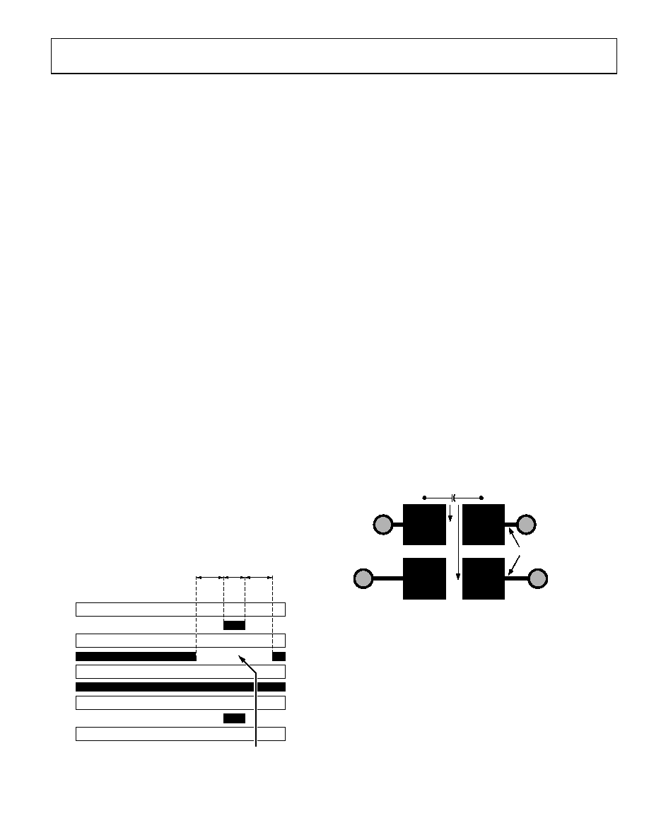
board stackup is shown in Figure 22.
PCB DIELECTRIC
LAYER 1: SIGNAL (MICROSTRIP)
SILKSCREEN
PCB DIELECTRIC
LAYER 2: GND (REFERENCE PLANE)
LAYER 3: PWR (REFERENCE PLANE)
LAYER 4: SIGNAL (MICROSTRIP)
W
3W
REFERENCE LAYER
RELIEVED UNDERNEATH
MICROSTRIP
07
00
4-
0
13
Figure 22. Example Board Stackup
HPD is a dc signal presented by a sink to a source to indicate
that the source EDID is available for reading. The placement
of this signal is not critical, but it should be routed as directly
as possible.
Power Supplies
The AD8194 has three separate power supplies referenced to
a single ground. The supply/ground pairs are
AVCC/AVEE
VTTI/AVEE
VTTO/AVEE
The AVCC/AVEE (3.3 V) supply powers the core of the
AD8194. The VTTI/AVEE supply (3.3 V) powers the input
termination (see Figure 19). Similarly, the VTTO/AVEE
supply (3.3 V) powers the output termination (see Figure 20).
In a typical application, all pins labeled AVEE should be con-
nected directly to ground. All pins labeled AVCC, VTTI, or
VTTO should be connected to 3.3 V. The supplies can also be
powered individually, but care must be taken to ensure that
each stage of the AD8194 is powered correctly.
Power Supply Bypassing
The AD8194 requires minimal supply bypassing. When
powering the supplies individually, place a 0.01 μF capacitor
between each 3.3 V supply pin (AVCC, VTTI, and VTTO) and
ground to filter out supply noise. Generally, bypass capacitors
should be placed near the power pins and should connect directly
to the relevant supplies (without long intervening traces). For
example, to minimize the parasitic inductance of the power
supply decoupling capacitors, minimize the trace length between
capacitor landing pads and the vias as shown in Figure 23.
EXTRA ADDED INDUCTANCE
RECOMMENDED
NOT RECOMMENDED
0
7004-
014
Figure 23. Recommended Pad Outline for Bypass Capacitors
In applications where the AD8194 is powered by a single 3.3 V
supply, it is recommended to use two reference supply planes
and bypass the 3.3 V reference plane to the ground reference
plane with one 220 pF, one 1000 pF, two 0.01 μF, and one 4.7 μF
capacitors. The capacitors should via down directly to the supply
planes and be placed within a few centimeters of the AD8194.
相关PDF资料 |
PDF描述 |
|---|---|
| AD8195ACPZ | IC BUFF HDMI/DVI W/EQUAL 40LFCSP |
| AD8196ACPZ | IC SWITCH DVI/HDMI 2:1 56-LFCSP |
| AD8197AASTZ | IC HDMI/DVI SWITCH 4:1 100LQFP |
| AD8197ASTZ-RL | IC SWITCH DVI/HDMI 4:1 100-LQFP |
| AD8197BASTZ-RL | IC SWITCH DVI/HDMI 4:1 100-LQFP |
相关代理商/技术参数 |
参数描述 |
|---|---|
| AD8194-EVALZ | 制造商:Analog Devices 功能描述:EVAL BD FOR AD8194 - Bulk |
| AD8195ACPZ | 功能描述:IC BUFF HDMI/DVI W/EQUAL 40LFCSP RoHS:是 类别:集成电路 (IC) >> 接口 - 模拟开关,多路复用器,多路分解器 系列:- 其它有关文件:STG4159 View All Specifications 标准包装:5,000 系列:- 功能:开关 电路:1 x SPDT 导通状态电阻:300 毫欧 电压电源:双电源 电压 - 电源,单路/双路(±):±1.65 V ~ 4.8 V 电流 - 电源:50nA 工作温度:-40°C ~ 85°C 安装类型:表面贴装 封装/外壳:7-WFBGA,FCBGA 供应商设备封装:7-覆晶 包装:带卷 (TR) |
| AD8195ACPZ-R7 | 功能描述:IC BUFF HDMI/DVI W/EQUAL 40LFCSP RoHS:是 类别:集成电路 (IC) >> 接口 - 模拟开关,多路复用器,多路分解器 系列:- 标准包装:1,000 系列:- 功能:多路复用器 电路:1 x 4:1 导通状态电阻:- 电压电源:双电源 电压 - 电源,单路/双路(±):±5V 电流 - 电源:7mA 工作温度:-40°C ~ 85°C 安装类型:表面贴装 封装/外壳:16-SOIC(0.154",3.90mm 宽) 供应商设备封装:16-SOIC 包装:带卷 (TR) |
| AD8195-EVALZ | 制造商:Analog Devices 功能描述:EVALUATION BOARD - Boxed Product (Development Kits) |
| AD8195XCPZ | 功能描述:IC BUFF HDMI/DVI W/EQUAL 40LFCSP 制造商:analog devices inc. 系列:- 包装:托盘 零件状态:上次购买时间 类型:HDMI/DVI 缓冲器 应用:HDTV 安装类型:表面贴装 封装/外壳:40-VFQFN 裸露焊盘,CSP 供应商器件封装:40-LFCSP-VQ(6x6) 标准包装:1 |
发布紧急采购,3分钟左右您将得到回复。