- 您现在的位置:买卖IC网 > PDF目录4590 > AD8196ACPZ-RL (Analog Devices Inc)IC SWITCH DVI/HDMI 2:1 56-LFCSP PDF资料下载
参数资料
| 型号: | AD8196ACPZ-RL |
| 厂商: | Analog Devices Inc |
| 文件页数: | 15/24页 |
| 文件大小: | 0K |
| 描述: | IC SWITCH DVI/HDMI 2:1 56-LFCSP |
| 标准包装: | 2,500 |
| 类型: | HDMI/DVI 开关 |
| 应用: | DVI,HDMI 信号开关 |
| 安装类型: | 表面贴装 |
| 封装/外壳: | 56-VFQFN 裸露焊盘,CSP |
| 供应商设备封装: | 56-LFCSP-VQ(8x8) |
| 包装: | 带卷 (TR) |
AD8196
Rev. 0 | Page 22 of 24
maximum allowed voltage on the auxiliary lines. For example,
if the DDC bus is using 5 V I2C, then AMUXVCC should be
connected to +5 V relative to DVEE.
In a typical application, all pins labeled AVEE or DVEE should
be connected directly to ground. All pins labeled AVCC,
DVCC, VTTI, or VTTO should be connected to 3.3 V, and
Pin AMUXVCC tied to 5 V. The supplies can also be powered
individually, but care must be taken to ensure that each stage of
the AD8196 is powered correctly.
Power Supply Bypassing
The AD8196 requires minimal supply bypassing. When
powering the supplies individually, place a 0.01 μF capacitor
between each 3.3 V supply pin (AVCC, DVCC, VTTI, and
VTTO) and ground to filter out supply noise. Generally, bypass
capacitors should be placed near the power pins and should
connect directly to the relevant supplies (without long inter-
vening traces). For example, to improve the parasitic inductance
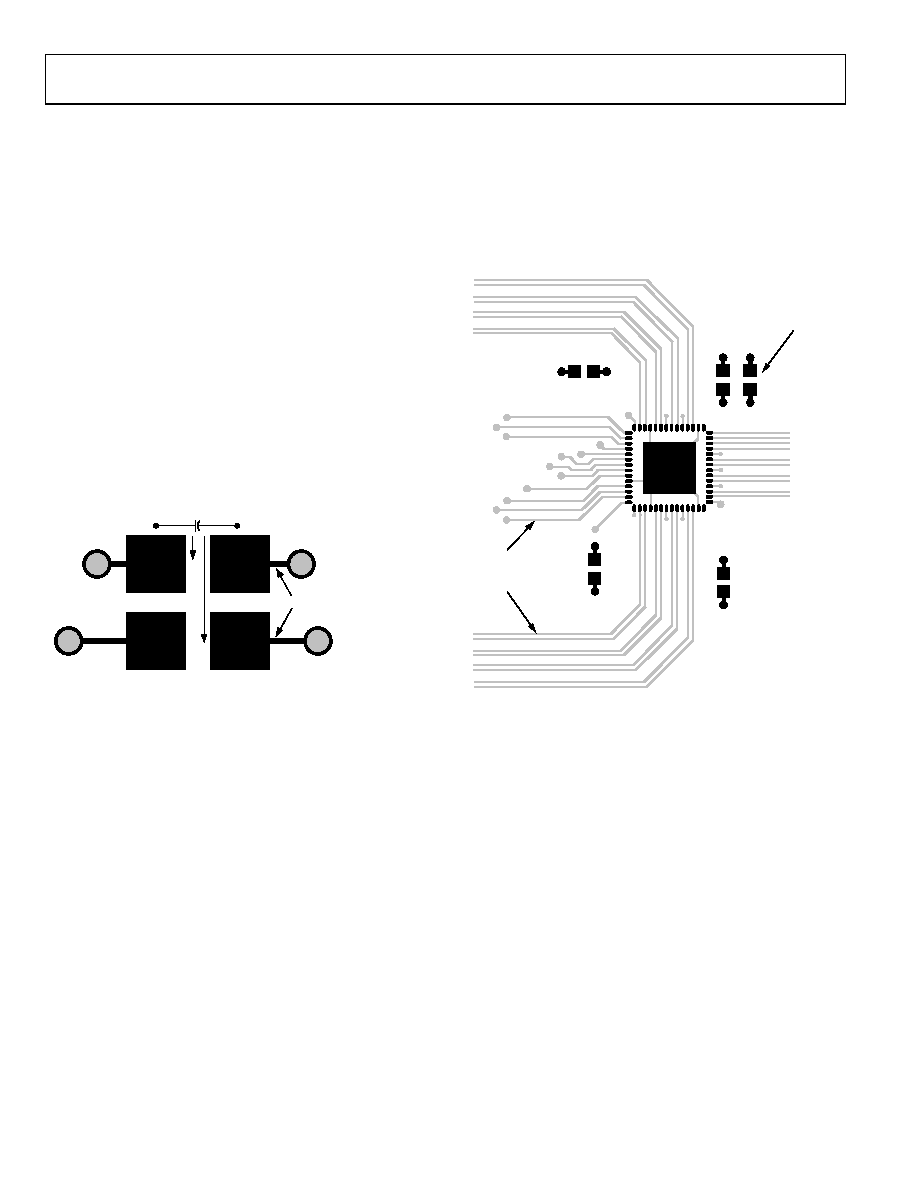
of the power supply decoupling capacitors, minimize the trace
length between capacitor landing pads and the vias as shown in
EXTRA ADDED INDUCTANCE
RECOMMENDED
NOT RECOMMENDED
064
70
-03
4
Figure 34. Recommended Pad Outline for Bypass Capacitors
In applications where the AD8196 is powered by a single 3.3 V
supply, it is recommended to use two reference supply planes
and bypass the 3.3 V reference plane to the ground reference
plane with one 220 pF, one 1000 pF, two 0.01 μF, and one 4.7 μF
capacitors. The capacitors should via down directly to the
supply planes and be placed within a few centimeters of the
AD8196. The AMUXVCC supply does not require additional
bypassing. This scheme is illustrated in Figure 35.
DECOUPLING
CAPACITORS
AUXILIARY LINES
TMDS TRACES
AD8196
0
64
70
-03
5
Figure 35. Example Placement of Power Supply Decoupling Capacitors
Around the AD8196
相关PDF资料 |
PDF描述 |
|---|---|
| AD8190ACPZ-R7 | IC SW HDMI/DVI 2:1 EQUAL 56LFCSP |
| LFEC6E-3QN208I | IC FPGA 6.1KLUTS 208PQFP |
| LFEC6E-4QN208C | IC FPGA 6.1KLUTS 147I/O 208-PQFP |
| LFEC6E-3FN484I | IC FPGA 6.1KLUTS 484FPBGA |
| LFEC6E-4FN484C | IC FPGA 6.1KLUTS 484FPBGA |
相关代理商/技术参数 |
参数描述 |
|---|---|
| AD8196-EVAL | 制造商:AD 制造商全称:Analog Devices 功能描述:2:1 HDMI/DVI Switch with Equalization |
| AD8197 | 制造商:AD 制造商全称:Analog Devices 功能描述:4:1 HDMI/DVI Switch with Equalization |
| AD8197A | 制造商:AD 制造商全称:Analog Devices 功能描述:4:1 HDMI/DVI Switch with Equalization |
| AD8197A_07 | 制造商:AD 制造商全称:Analog Devices 功能描述:4:1 HDMI/DVI Switch with Equalization |
| AD8197AASTZ | 功能描述:IC HDMI/DVI SWITCH 4:1 100LQFP RoHS:是 类别:集成电路 (IC) >> 接口 - 模拟开关,多路复用器,多路分解器 系列:- 其它有关文件:STG4159 View All Specifications 标准包装:5,000 系列:- 功能:开关 电路:1 x SPDT 导通状态电阻:300 毫欧 电压电源:双电源 电压 - 电源,单路/双路(±):±1.65 V ~ 4.8 V 电流 - 电源:50nA 工作温度:-40°C ~ 85°C 安装类型:表面贴装 封装/外壳:7-WFBGA,FCBGA 供应商设备封装:7-覆晶 包装:带卷 (TR) |
发布紧急采购,3分钟左右您将得到回复。