参数资料
| 型号: | AD8203YRMZ |
| 厂商: | Analog Devices Inc |
| 文件页数: | 4/20页 |
| 文件大小: | 0K |
| 描述: | IC AMP DIFF 60KHZ 8MSOP |
| 标准包装: | 50 |
| 放大器类型: | 差分 |
| 电路数: | 1 |
| 转换速率: | 0.330 V/µs |
| 增益带宽积: | 60kHz |
| 电流 - 输入偏压: | 40nA |
| 电压 - 输入偏移: | 2000µV |
| 电流 - 电源: | 250µA |
| 电压 - 电源,单路/双路(±): | 3.5 V ~ 12 V |
| 工作温度: | -40°C ~ 125°C |
| 安装类型: | 表面贴装 |
| 封装/外壳: | 8-TSSOP,8-MSOP(0.118",3.00mm 宽) |
| 供应商设备封装: | 8-MSOP |
| 包装: | 管件 |
| 产品目录页面: | 765 (CN2011-ZH PDF) |
AD8203
Data Sheet
Rev. D | Page 12 of 20
THEORY OF OPERATION
The AD8203 consists of a preamp and buffer, arranged as
shown in Figure 40. Like-named resistors have equal values.
The preamp incorporates a dynamic bridge (subtractor) circuit.
Identical networks (within the shaded areas) consisting of RA,
RB, RC, and RG, attenuate input signals applied to Pin 1 and
Pin 8. Note that when equal amplitude signals are asserted at
Input 1 and Input 8, and the output of A1 is equal to the
common potential (that is, 0), the two attenuators form a
balanced-bridge network. When the bridge is balanced, the
differential input voltage at A1, and thus its output, is 0.
Any common-mode voltage applied to both inputs keeps the
bridge balanced and the A1 output at 0. Because the resistor
networks are carefully matched, the common-mode signal
rejection approaches this ideal state.
However, if the signals applied to the inputs differ, the result is a
difference at the input to A1. A1 responds by adjusting its output
to drive RB, by way of RG, to adjust the voltage at its inverting
input until it matches the voltage at its noninverting input.
By attenuating voltages at Pin 1 and Pin 8, the amplifier inputs
are held within the power supply range, even if Pin 1 and Pin 8
input levels exceed the supply or fall below common (ground).
The input network also attenuates normal (differential) mode
voltages. RC and RG form an attenuator that scales A1 feedback,
forcing large output signals to balance relatively small differen-
tial inputs. The resistor ratios establish the preamp gain at 7.
Because the differential input signal is attenuated and then
amplified to yield an overall gain of 7, Amplifier A1 operates at
a higher noise gain, multiplying deficiencies such as input offset
voltage and noise with respect to Pin 1 and Pin 8.
A1
A3
RCM
(TRIMMED)
100k
RA
–IN
RG
RC
RB
RA
RC
RB
RG
+IN
COM
A2
RF
AD8203
5
4
3
1
2
8
05013-014
Figure 40. Simplified Schematic
To minimize these errors while extending the common-mode
range, a dedicated feedback loop is used to reduce the range of
common-mode voltage applied to A1 for a given overall range
at the inputs. By offsetting the range of voltage applied to the
compensator, the input common-mode range is also offset to
include voltages more negative than the power supply. The
A3 amplifier detects the common-mode signal applied to A1
and adjusts the voltage on the matched RCM resistors to reduce
the common-mode voltage range at the A1 inputs. By adjusting
the common voltage of these resistors, the common-mode input
range is extended while, at the same time, the normal mode
signal attenuation is reduced, leading to better performance
referred to input.
The output of the dynamic bridge taken from A1 is connected
to Pin 3 by way of a 100 k series resistor, provided for low-
pass filtering and gain adjustment. The resistors in the input
networks of the preamp and the buffer feedback resistors are
ratio-trimmed for high accuracy.
The output of the preamp drives a gain-of-2 buffer amplifier,
A2, implemented with carefully matched feedback resistors RF.
The 2-stage system architecture of the AD8203 enables the user
to incorporate a low-pass filter prior to the output buffer. By
separating the gain into two stages, a full-scale, rail-to-rail
signal from the preamp can be filtered at Pin 3, and a half-scale
signal, resulting from filtering, can be restored to full scale by
the output buffer amp. The source resistance seen by the
inverting input of A2 is approximately 100 k to minimize the
effects of the input bias current of A2. However, this current is
quite small, and errors resulting from applications that
mismatch the resistance are correspondingly small.
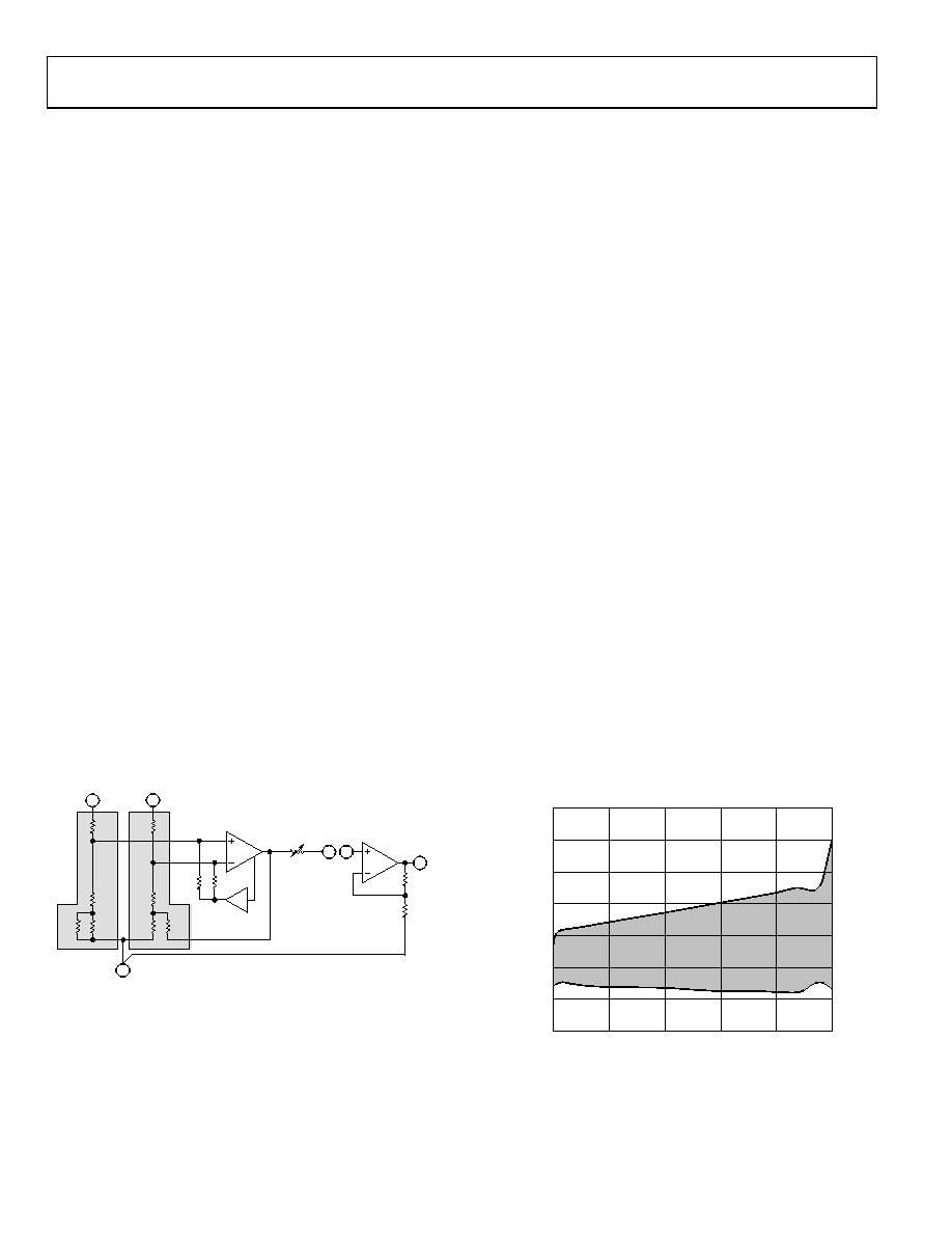
The A2 input bias current has a typical value of 40 nA, however,
this can increase under certain conditions. For example, if the
input signal to the A2 amplifier is VCC/2, the output attempts to
go to VCC due to the gain of 2. However, the output saturates
because the maximum specified voltage for correct operation is
200 mV below VCC. Under these conditions the total input bias
current increases (see Figure 41 for more information).
DIFFERENTIAL MODE VOLTAGE (V)
A2
INPUT
BIAS
CURRENT
(nA)
–140
0
05013-035
–120
–100
–80
–60
–40
–20
0.5
0
1.0
1.5
2.0
2.5
Figure 41. A2 Input Bias Current vs. Input Voltage and Temperature. The
Shaded Area Is the Bias Current from 40°C to +125°C.
相关PDF资料 |
PDF描述 |
|---|---|
| KD1245PFS2 H | FAN 12VDC 45X10MM 1.2W 7.1CFM |
| KD1205PFB2 H | FAN 12VDC 50X10.5MM 1.2W 9.5CFM |
| LT1006CN8#PBF | IC PREC OP-AMP 5V SINGLE 8-DIP |
| AD8039ARZ | IC OPAMP VF DUAL LP LN 8SOIC |
| KD1204PFS3 H | FAN 12VDC 40X10.5MM .7W 4.2CFM |
相关代理商/技术参数 |
参数描述 |
|---|---|
| AD8203YRMZ-R7 | 功能描述:IC AMP DIFF 60KHZ 8MSOP RoHS:是 类别:集成电路 (IC) >> Linear - Amplifiers - Instrumentation 系列:- 标准包装:1,000 系列:- 放大器类型:电压反馈 电路数:4 输出类型:满摆幅 转换速率:33 V/µs 增益带宽积:20MHz -3db带宽:30MHz 电流 - 输入偏压:2nA 电压 - 输入偏移:3000µV 电流 - 电源:2.5mA 电流 - 输出 / 通道:30mA 电压 - 电源,单路/双路(±):4.5 V ~ 16.5 V,±2.25 V ~ 8.25 V 工作温度:-40°C ~ 85°C 安装类型:表面贴装 封装/外壳:14-SOIC(0.154",3.90mm 宽) 供应商设备封装:14-SOIC 包装:带卷 (TR) |
| AD8203YRMZ-RL | 功能描述:IC AMP DIFF 60KHZ 8MSOP RoHS:是 类别:集成电路 (IC) >> Linear - Amplifiers - Instrumentation 系列:- 标准包装:2,500 系列:- 放大器类型:通用 电路数:1 输出类型:满摆幅 转换速率:0.11 V/µs 增益带宽积:350kHz -3db带宽:- 电流 - 输入偏压:4nA 电压 - 输入偏移:20µV 电流 - 电源:260µA 电流 - 输出 / 通道:20mA 电压 - 电源,单路/双路(±):2.7 V ~ 36 V,±1.35 V ~ 18 V 工作温度:-40°C ~ 85°C 安装类型:表面贴装 封装/外壳:8-SOIC(0.154",3.90mm 宽) 供应商设备封装:8-SO 包装:带卷 (TR) |
| AD8203YRZ | 功能描述:IC AMP DIFF 60KHZ 8SOIC RoHS:是 类别:集成电路 (IC) >> Linear - Amplifiers - Instrumentation 系列:- 产品培训模块:Differential Circuit Design Techniques for Communication Applications 标准包装:1 系列:- 放大器类型:RF/IF 差分 电路数:1 输出类型:差分 转换速率:9800 V/µs 增益带宽积:- -3db带宽:2.9GHz 电流 - 输入偏压:3µA 电压 - 输入偏移:- 电流 - 电源:40mA 电流 - 输出 / 通道:- 电压 - 电源,单路/双路(±):3 V ~ 3.6 V 工作温度:-40°C ~ 85°C 安装类型:表面贴装 封装/外壳:16-VQFN 裸露焊盘,CSP 供应商设备封装:16-LFCSP-VQ 包装:剪切带 (CT) 产品目录页面:551 (CN2011-ZH PDF) 其它名称:ADL5561ACPZ-R7CT |
| AD8203YRZ-R7 | 功能描述:IC AMP DIFF 60KHZ 8SOIC RoHS:是 类别:集成电路 (IC) >> Linear - Amplifiers - Instrumentation 系列:- 标准包装:1,000 系列:- 放大器类型:电压反馈 电路数:4 输出类型:满摆幅 转换速率:33 V/µs 增益带宽积:20MHz -3db带宽:30MHz 电流 - 输入偏压:2nA 电压 - 输入偏移:3000µV 电流 - 电源:2.5mA 电流 - 输出 / 通道:30mA 电压 - 电源,单路/双路(±):4.5 V ~ 16.5 V,±2.25 V ~ 8.25 V 工作温度:-40°C ~ 85°C 安装类型:表面贴装 封装/外壳:14-SOIC(0.154",3.90mm 宽) 供应商设备封装:14-SOIC 包装:带卷 (TR) |
| AD8203YRZ-RL | 功能描述:IC AMP DIFF 60KHZ 8SOIC RoHS:是 类别:集成电路 (IC) >> Linear - Amplifiers - Instrumentation 系列:- 标准包装:2,500 系列:- 放大器类型:通用 电路数:1 输出类型:满摆幅 转换速率:0.11 V/µs 增益带宽积:350kHz -3db带宽:- 电流 - 输入偏压:4nA 电压 - 输入偏移:20µV 电流 - 电源:260µA 电流 - 输出 / 通道:20mA 电压 - 电源,单路/双路(±):2.7 V ~ 36 V,±1.35 V ~ 18 V 工作温度:-40°C ~ 85°C 安装类型:表面贴装 封装/外壳:8-SOIC(0.154",3.90mm 宽) 供应商设备封装:8-SO 包装:带卷 (TR) |
发布紧急采购,3分钟左右您将得到回复。