- 您现在的位置:买卖IC网 > PDF目录373941 > AD8203YRZ-RL (ANALOG DEVICES INC) High Common-Mode Voltage, Single-Supply Difference Amplifier PDF资料下载
参数资料
| 型号: | AD8203YRZ-RL |
| 厂商: | ANALOG DEVICES INC |
| 元件分类: | 运动控制电子 |
| 英文描述: | High Common-Mode Voltage, Single-Supply Difference Amplifier |
| 中文描述: | OP-AMP, 1000 uV OFFSET-MAX, PDSO8 |
| 封装: | LEAD FREE, MS-012AA, SOIC-8 |
| 文件页数: | 16/20页 |
| 文件大小: | 239K |
| 代理商: | AD8203YRZ-RL |
AD8203
Rev. B | Page 16 of 20
40log (f
2
/f
1
)
f
1
A
f
2
f
22
/f
1
FREQUENCY
A 1-POLE FILTER, CORNER f
1
, AND
A 2-POLE FILTER, CORNER f
, HAVE
THE SAME ATTENUATION –40log (f
2
/f
1
)
AT FREQUENCY f
22
/f
1
20dB/DECADE
40dB/DECADE
0
Figure 49
by a 1-pole low-pass filter, shown in
frequency of 3.6 Hz, which provides about 30 dB of attenuation
at 100 Hz. A higher rate of attenuation can be obtained using a
2-pole filter with f
this circuit uses two separate capacitors, the total capacitance is
less than half that needed for the 1-pole filter.
, set with a corner
Figure 48. Comparative Responses of 1-Pole and 2-Pole Low-Pass Filters
HIGH LINE CURRENT SENSING WITH LPF AND
GAIN ADJUSTMENT
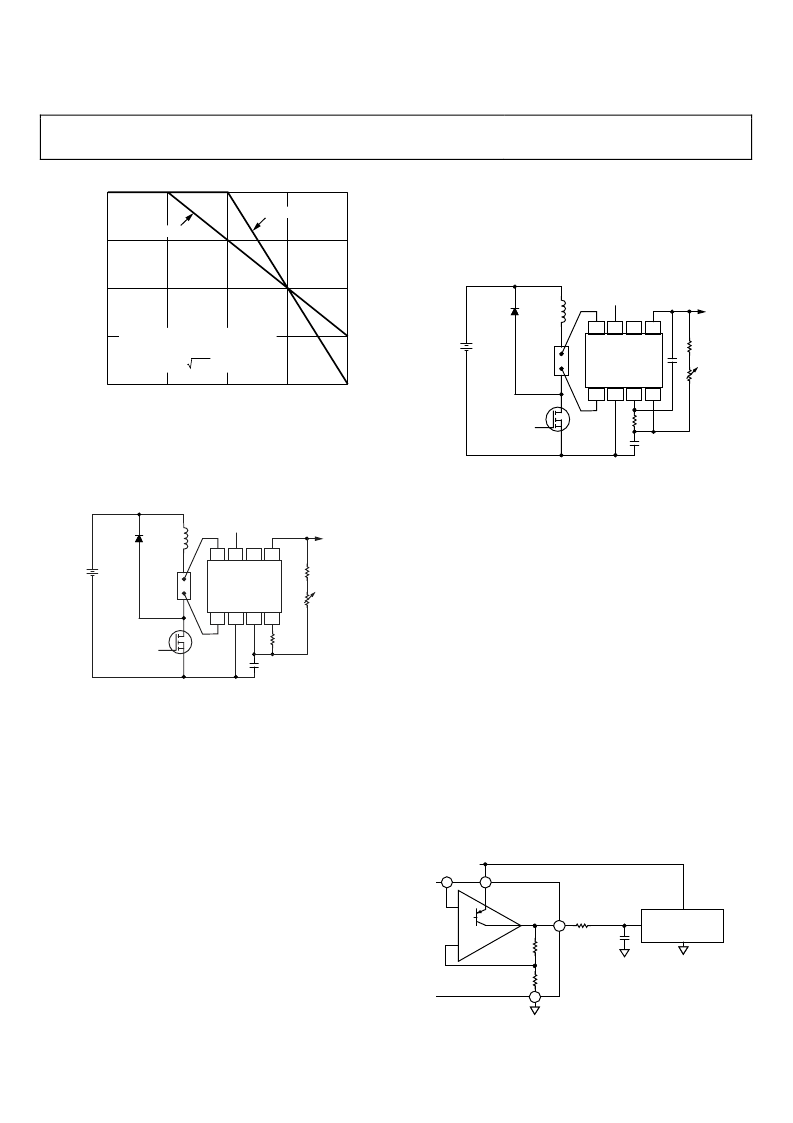
Figure 49 is another refinement of Figure 2, including gain
adjustment and low-pass filtering.
GND
NC
–IN
+IN
A1
+V
S
A2
OUT
AD8203
5V
INDUCTIVE
LOAD
POWER
DEVICE
4-TERM
SHUNT
CLAMP
DIODE
BATTERY
14V
NC = NO CONNECT
COMMON
0
C
OUT
4V/AMP
5% CALIBRATION RANGE
f
(Hz) = 0.767Hz/C(
μ
F)
(0.22
μ
F FOR f
C
= 3.6Hz)
V
NULL
133k
Ω
20k
Ω
Figure 49. High Line Current Sensor Interface;
Gain = ×40, Single-Pole Low-Pass Filter
A power device that is either on or off controls the current in
the load. The average current is proportional to the duty cycle
of the input pulse and is sensed by a small value resistor. The
average differential voltage across the shunt is typically 100 mV,
although its peak value is higher by an amount that depends on
the inductance of the load and the control frequency. The
common-mode voltage, conversely, extends from roughly 1 V
above ground for the on condition to about 1.5 V above the
battery voltage for the off condition. The conduction of the
clamping diode regulates the common-mode potential applied
to the device. For example, a battery spike of 20 V may result in
an applied common-mode potential of 21.5 V to the input of
the devices.
To produce a full-scale output of 4 V, a gain ×40 is used, adjust-
able by ±5% to absorb the tolerance in the shunt. There is
sufficient headroom to allow 10% overrange (to 4.4 V). The
roughly triangular voltage across the sense resistor is averaged
C
= 20 Hz, as shown in Figure 50. Although
GND
NC
–IN
+IN
A1
+V
S
A2
OUT
AD8203
5V
INDUCTIVE
LOAD
POWER
DEVICE
4-TERM
SHUNT
CLAMP
DIODE
BATTERY
14V
NC = NO CONNECT
COMMON
0
f
(Hz) = 1/C(
μ
F)
(0.05
μ
F FOR f
C
= 20Hz)
C
OUTPUT
93k
Ω
C
301k
Ω
50k
Ω
Figure 50. 2-Pole Low-Pass Filter
DRIVING CHARGE REDISTRIBUTION ADCS
When driving CMOS ADCs, such as those embedded in popu-
lar microcontrollers, the charge injection (ΔQ) can cause a
significant deflection in the output voltage of the AD8203.
Though generally of short duration, this deflection may persist
until after the sample period of the ADC has expired due to the
relatively high open-loop output impedance (21 kΩ) of the
AD8203. Including an R-C network in the output can signifi-
cantly reduce the effect. The capacitor helps to absorb the
transient charge, effectively lowering the high frequency output
impedance of the AD8203. For these applications, the output
signal should be taken from the midpoint of the
R
LAG
to C
LAG
combination, as shown in Figure 51.
Since the perturbations from the analog-to-digital converter are
small, the output impedance of the AD8203 appears to be low. The
transient response, therefore, has a time constant governed by the
product of the two LAG components, C
LAG
× R
LAG
. For the values
shown in Figure 51, this time constant is programmed at approxi-
mately 10 μs. Therefore, if samples are taken at several tens of
microseconds or more, there is negligible charge stack-up.
+IN
–IN
10k
Ω
10k
Ω
AD8203
5V
R
LAG
1k
Ω
C
LAG
0.01
μ
F
MICROPROCESSOR
A/D
A2
2
4
7
5
0
Figure 51. Recommended Circuit for Driving CMOS A/D
相关PDF资料 |
PDF描述 |
|---|---|
| AD8205YCSURF | Zero Drift, Digitally Programmable Instrumentation Amplifier; Package: LFCSP (4x4x.85mm, 2.10mm exposed pad); No of Pins: 16; Temperature Range: Industrial |
| AD8205YR-REEL | Single-Supply 42 V System Difference Amplifier |
| AD8205YR-REEL7 | 10 MHz, 20 V/µs, G = 1, 2, 4, 8 iCMOS® Programmable Gain Instrumentation Amplifier; Package: EVALUATION BOARDS; No of Pins: -; Temperature Range: Industrial |
| AD8205 | Single-Supply 42 V System Difference Amplifier |
| AD8205YR | +3.3V, 2.5Gbps/2.7Gbps, SDH/SONET 4:1 Serializer with Clock Synthesis |
相关代理商/技术参数 |
参数描述 |
|---|---|
| AD8205 | 制造商:AD 制造商全称:Analog Devices 功能描述:Single-Supply 42 V System Difference Amplifier |
| AD8205AR | 制造商:Analog Devices 功能描述:- Bulk |
| AD8205WHRZ | 制造商:Analog Devices 功能描述:42VSNGLSUPPLYDIFFAMP - Rail/Tube 制造商:Analog Devices 功能描述:IC OPAMP DIFF 50KHZ 8SOIC 制造商:Analog Devices 功能描述:42V Sngl Supply Diff Amp |
| AD8205WHRZ-RL | 制造商:Analog Devices 功能描述:42VSNGLSUPPLYDIFFAMP - Tape and Reel 制造商:Analog Devices 功能描述:IC OPAMP DIFF 50KHZ 8SOIC 制造商:Analog Devices 功能描述:42V Sngl Supply Diff Amp |
| AD8205WYRZ | 功能描述:IC AMP DIFF 42V SGL 8SOIC RoHS:是 类别:集成电路 (IC) >> Linear - Amplifiers - Instrumentation 系列:- 标准包装:100 系列:- 放大器类型:通用 电路数:1 输出类型:- 转换速率:0.2 V/µs 增益带宽积:- -3db带宽:- 电流 - 输入偏压:100pA 电压 - 输入偏移:30µV 电流 - 电源:380µA 电流 - 输出 / 通道:- 电压 - 电源,单路/双路(±):±2 V ~ 18 V 工作温度:0°C ~ 70°C 安装类型:表面贴装 封装/外壳:8-SOIC(0.154",3.90mm 宽) 供应商设备封装:8-SO 包装:管件 |
发布紧急采购,3分钟左右您将得到回复。