参数资料
| 型号: | AD8205YRZ-RL |
| 厂商: | Analog Devices Inc |
| 文件页数: | 12/12页 |
| 文件大小: | 0K |
| 描述: | IC AMP DIFF 8SOIC |
| 产品培训模块: | Current Sense Amplifiers |
| 标准包装: | 2,500 |
| 放大器类型: | 差分 |
| 电路数: | 1 |
| 转换速率: | 0.5 V/µs |
| -3db带宽: | 50kHz |
| 电压 - 输入偏移: | 2000µV |
| 电流 - 电源: | 2mA |
| 电压 - 电源,单路/双路(±): | 4.5 V ~ 5.5 V |
| 工作温度: | -40°C ~ 125°C |
| 安装类型: | 表面贴装 |
| 封装/外壳: | 8-SOIC(0.154",3.90mm 宽) |
| 供应商设备封装: | 8-SO |
| 包装: | 带卷 (TR) |
Data Sheet
AD8205
Rev. | Page 9 of 12
OUTPUT OFFSET ADJUSTMENT
The output of the AD8205 can be adjusted for unidirectional or
bidirectional operation.
UNIDIRECTIONAL OPERATION
Unidirectional operation allows the AD8205 to measure
currents through a resistive shunt in one direction. The basic
modes for unidirectional operation are ground referenced
output mode and V+ referenced output mode.
In the case of unidirectional operation, the output could be set
at the negative rail (near ground) or at the positive rail (near
V+) when the differential input is 0 V. The output moves to the
opposite rail when a correct polarity differential input voltage is
applied. In this case, full scale is approximately 100 mV. The
required polarity of the differential input depends on the output
voltage setting. If the output is set at the positive rail, the input
polarity needs to be negative to move the output down. If the
output is set at ground, the polarity is positive to move the
output up.
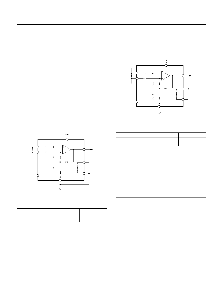
GROUND REFERENCED OUTPUT
When using the AD8205 in this mode, both reference inputs are
tied to ground, which causes the output to sit at the negative rail
when there are zero differential volts at the input (see Figure 14).
04315-0-013
AD8205
+IN
–IN
NC
NC = NO CONNECT
GND
V+
OUT
VREF1
VREF2
Figure 14. Ground Referenced Output
Table 4. V+ = 5 V
VIN (Referred to IN)
VO
0 V
0.05 V
100 mV
4.8 V
V+ REFERENCED OUTPUT
This mode is set when both reference pins are tied to the
positive supply. It is typically used when the diagnostic scheme
requires detection of the amplifier and the wiring before power
is applied to the load (see Figure 15).
04315-0-014
AD8205
+IN
–IN
NC
NC = NO CONNECT
GND
V+
OUT
VREF1
VREF2
Figure 15. V+ Referenced Output
Table 5. V+ = 5 V
VIN (Referred to IN)
VO
0 V
4.8 V
100 mV
0.05 V
BIDIRECTIONAL OPERATION
Bidirectional operation allows the AD8205 to measure currents
through a resistive shunt in two directions.
In this case, the output is set anywhere within the output range.
Typically, it is set at half-scale for equal range in both directions.
In some cases, however, it is set at a voltage other than half-scale
when the bidirectional current is nonsymmetrical.
Table 6. V+ = 5 V, VO = 2.5 with VIN = 0 V
VIN (Referred to IN)
VO
+40 mV
4.5 V
40 mV
0.5 V
Adjusting the output is accomplished by applying voltage(s) to
the reference inputs.
VREF1 and VREF2 are tied to internal resistors that connect to an
internal offset node. There is no operational difference between
the pins.
D
相关PDF资料 |
PDF描述 |
|---|---|
| KTR10EZPF1003 | RES 100K OHM 1/8W 1% 0805 SMD |
| AD8616ARZ-REEL | IC OPAMP GP R-R CMOS 24MHZ 8SOIC |
| AD8007ARZ-RL | IC OPAMP CF ULDIST LN LP 8SOIC |
| MMA23-0201P1 | CONN RACK/PANEL 20POS 5A |
| OP282GSZ-REEL7 | IC OPAMP JFET 4MHZ DUAL LP 8SOIC |
相关代理商/技术参数 |
参数描述 |
|---|---|
| AD8206 | 制造商:AD 制造商全称:Analog Devices 功能描述:Single-Supply, 42 V System Difference Amplifier |
| AD8206_05 | 制造商:AD 制造商全称:Analog Devices 功能描述:Single-Supply, 42 V System Difference Amplifier |
| AD8206_12 | 制造商:AD 制造商全称:Analog Devices 功能描述:High Common-Mode Voltage, Bidirectional Current Shunt Amplifier |
| AD8206AR | 制造商:Analog Devices 功能描述:SINGLE SUPPLY 42V SYSTEM DIFFERENCE AMPLIFIER - Bulk |
| AD8206WHRZ | 功能描述:差分放大器 SGL-Supply 42V Systm RoHS:否 制造商:Analog Devices 通道数量:1 Channel 带宽:900 MHz 可用增益调整:5.6 dB to 20 dB 输入补偿电压:1 mV at 5 V 共模抑制比(最小值):67 dB 工作电源电压:11 V 电源电流:28 mA 最大工作温度:+ 85 C 最小工作温度:- 40 C 安装风格:SMD/SMT 封装 / 箱体:SOIC-8 封装:Reel |
发布紧急采购,3分钟左右您将得到回复。