参数资料
| 型号: | AD820ARZ |
| 厂商: | Analog Devices Inc |
| 文件页数: | 9/24页 |
| 文件大小: | 0K |
| 描述: | IC OPAMP JFET R-R 1.8MHZ 8SOIC |
| 产品培训模块: | Pulse Oximetry Solutions Top Five Problems in Photodiode Opamp Circuits |
| 标准包装: | 98 |
| 放大器类型: | J-FET |
| 电路数: | 1 |
| 输出类型: | 满摆幅 |
| 转换速率: | 3 V/µs |
| 增益带宽积: | 1.8MHz |
| -3db带宽: | 1.9MHz |
| 电流 - 输入偏压: | 2pA |
| 电压 - 输入偏移: | 400µV |
| 电流 - 电源: | 700µA |
| 电流 - 输出 / 通道: | 20mA |
| 电压 - 电源,单路/双路(±): | 5 V ~ 36 V,±2.5 V ~ 18 V |
| 工作温度: | -40°C ~ 85°C |
| 安装类型: | 表面贴装 |
| 封装/外壳: | 8-SOIC(0.154",3.90mm 宽) |
| 供应商设备封装: | 8-SO |
| 包装: | 管件 |
| 产品目录页面: | 772 (CN2011-ZH PDF) |
AD820
Rev. H | Page 17 of 24
OUTPUT CHARACTERISTICS
The AD820 unique bipolar rail-to-rail output stage swings
within 5 mV of the negative supply and 10 mV of the positive
supply with no external resistive load. The approximate output
saturation resistance of the AD820 is 40 Ω sourcing and 20 Ω
sinking. This can be used to estimate output saturation voltage
when driving heavier current loads. For instance, when sourcing
5 mA, the saturation voltage to the positive supply rail is 200 mV;
when sinking 5 mA, the saturation voltage to the negative rail
is 100 mV.
The open-loop gain characteristic of the amplifier changes
as a function of resistive load, as shown in Figure 10 through
Figure 13. For load resistances over 20 kΩ, the AD820 input
error voltage is virtually unchanged until the output voltage is
driven to 180 mV of either supply.
If the AD820 output is driven hard against the output saturation
voltage, it recovers within 2 μs of the input returning to the
linear operating region of the amplifier.
Direct capacitive load interacts with the effective output imped-
ance of the amplifier to form an additional pole in the amplifier
feedback loop, which can cause excessive peaking on the pulse
response or loss of stability. The worst case occurs when the
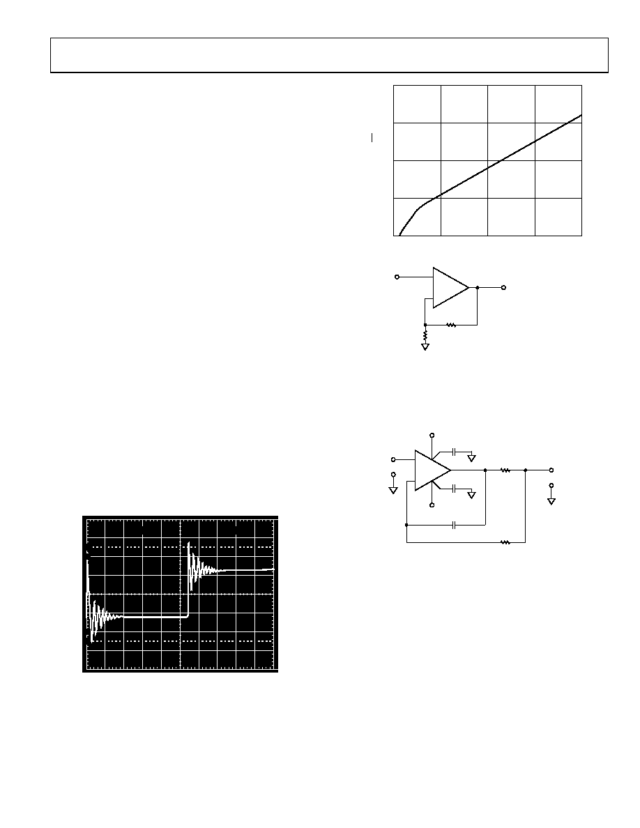
amplifier is used as a unity-gain follower. Figure 40 shows
AD820 pulse response as a unity-gain follower driving 350 pF.
This amount of overshoot indicates approximately 20 degrees
of phase margin—the system is stable, but is nearing the edge.
Configurations with less loop gain, and as a result less loop
bandwidth, are much less sensitive to capacitance load effects.
Figure 41 is a plot of noise gain vs. the capacitive load that results
in a 20 degree phase margin for the AD820. Noise gain is the
inverse of the feedback attenuation factor provided by the
feedback network in use.
00
87
3-
04
1
20mV
2s
100
90
10
0%
Figure 40. Small Signal Response of AD820 as Unity-Gain Follower Driving
350 pF Capacitive Load
00
87
3-
0
42
5
1
300
30k
CAPACITIVE LOAD FOR 20 PHASE MARGIN (pF)
N
OIS
E
GA
IN
(
1+
)
P
I
P
F
4
3
2
1k
3k
10k
–
+
RF
R1
Figure 41. Noise Gain vs. Capacitive Load Tolerance
Figure 42 shows a possible configuration for extending
capacitance load drive capability for a unity-gain follower. With
these component values, the circuit drives 5000 pF with a 10%
overshoot.
0
08
73
-04
3
AD820
–
+
–
+
+VS
–VS
0.01F
20pF
20k
100
VOUT
VIN
3
2
4
7
6
–
+
Figure 42. Extending Unity-Gain Follower Capacitive Load Capability
Beyond 350 pF
SINGLE-SUPPLY HALF-WAVE AND FULL-WAVE
RECTIFIERS
An AD820 configured as a unity-gain follower and operated
with a single supply can be used as a simple half-wave rectifier.
The AD820 inputs maintain picoamp level input currents even
when driven well below the negative supply. The rectifier puts
that behavior to good use, maintaining an input impedance of
over 1011 Ω for input voltages from 1 V from the positive supply
to 20 V below the negative supply.
The full- and half-wave rectifier shown in Figure 43 operates as
follows: when VIN is above ground, R1 is bootstrapped through
the unity-gain follower, A1, and the loop of Amplifier A2. This
forces the inputs of A2 to be equal; thus, no current flows through
R1 or R2, and the circuit output tracks the input. When VIN is
below ground, the output of A1 is forced to ground. The
相关PDF资料 |
PDF描述 |
|---|---|
| RMCF0402JT300R | RES TF 300 OHM 5% 1/16W 0402 |
| AD8132ARMZ-REEL7 | IC AMP DIFF LDIST LP 70MA 8MSOP |
| LT1413S8#PBF | IC PRECISION OP-AMP DUAL 8-SOIC |
| LTC6241HVCS8#PBF | IC OP AMP DUAL R-R 8-SOIC |
| RMCF0402JT1M00 | RES 1M OHM 1/16W 5% 0402 SMD |
相关代理商/技术参数 |
参数描述 |
|---|---|
| AD820ARZ-REEL | 功能描述:IC OPAMP JFET R-R 1.8MHZ 8SOIC RoHS:是 类别:集成电路 (IC) >> Linear - Amplifiers - Instrumentation 系列:- 标准包装:50 系列:- 放大器类型:通用 电路数:2 输出类型:满摆幅 转换速率:1.8 V/µs 增益带宽积:6.5MHz -3db带宽:4.5MHz 电流 - 输入偏压:5nA 电压 - 输入偏移:100µV 电流 - 电源:65µA 电流 - 输出 / 通道:35mA 电压 - 电源,单路/双路(±):1.8 V ~ 5.25 V,±0.9 V ~ 2.625 V 工作温度:-40°C ~ 85°C 安装类型:表面贴装 封装/外壳:10-TFSOP,10-MSOP(0.118",3.00mm 宽) 供应商设备封装:10-MSOP 包装:管件 |
| AD820ARZ-REEL7 | 功能描述:IC OPAMP JFET R-R 1.8MHZ 8SOIC RoHS:是 类别:集成电路 (IC) >> Linear - Amplifiers - Instrumentation 系列:- 标准包装:50 系列:LinCMOS™ 放大器类型:通用 电路数:4 输出类型:- 转换速率:0.05 V/µs 增益带宽积:110kHz -3db带宽:- 电流 - 输入偏压:0.7pA 电压 - 输入偏移:210µV 电流 - 电源:57µA 电流 - 输出 / 通道:30mA 电压 - 电源,单路/双路(±):3 V ~ 16 V,±1.5 V ~ 8 V 工作温度:-40°C ~ 85°C 安装类型:表面贴装 封装/外壳:14-SOIC(0.154",3.90mm 宽) 供应商设备封装:14-SOIC 包装:管件 产品目录页面:865 (CN2011-ZH PDF) 其它名称:296-1834296-1834-5 |
| AD820BN | 制造商:AD 制造商全称:Analog Devices 功能描述:Single Supply, Rail to Rail Low Power FET-Input Op Amp |
| AD820BR | 功能描述:IC OPAMP JFET R-R 1.8MHZ 8SOIC RoHS:否 类别:集成电路 (IC) >> Linear - Amplifiers - Instrumentation 系列:- 标准包装:150 系列:- 放大器类型:音频 电路数:2 输出类型:- 转换速率:5 V/µs 增益带宽积:12MHz -3db带宽:- 电流 - 输入偏压:100nA 电压 - 输入偏移:500µV 电流 - 电源:6mA 电流 - 输出 / 通道:50mA 电压 - 电源,单路/双路(±):4 V ~ 32 V,±2 V ~ 16 V 工作温度:-40°C ~ 85°C 安装类型:表面贴装 封装/外壳:8-TSSOP(0.173",4.40mm 宽) 供应商设备封装:8-TSSOP 包装:管件 |
| AD820BR-REEL | 功能描述:IC OPAMP JFET R-R 1.8MHZ 8SOIC RoHS:否 类别:集成电路 (IC) >> Linear - Amplifiers - Instrumentation 系列:- 标准包装:50 系列:- 放大器类型:J-FET 电路数:2 输出类型:- 转换速率:3.5 V/µs 增益带宽积:1MHz -3db带宽:- 电流 - 输入偏压:30pA 电压 - 输入偏移:2000µV 电流 - 电源:200µA 电流 - 输出 / 通道:- 电压 - 电源,单路/双路(±):7 V ~ 36 V,±3.5 V ~ 18 V 工作温度:0°C ~ 70°C 安装类型:通孔 封装/外壳:8-DIP(0.300",7.62mm) 供应商设备封装:8-PDIP 包装:管件 |
发布紧急采购,3分钟左右您将得到回复。