- 您现在的位置:买卖IC网 > PDF目录22244 > AD8212WYRMZ-R7 (Analog Devices Inc)IC CURRENT MONITOR 8MSOP PDF资料下载
参数资料
| 型号: | AD8212WYRMZ-R7 |
| 厂商: | Analog Devices Inc |
| 文件页数: | 9/16页 |
| 文件大小: | 0K |
| 描述: | IC CURRENT MONITOR 8MSOP |
| 标准包装: | 1,000 |
| 功能: | 电流监控器 |
| 检测方法: | 高端 |
| 输入电压: | 7 V ~ 65 V |
| 电流 - 输出: | 500µA |
| 工作温度: | -40°C ~ 125°C |
| 安装类型: | 表面贴装 |
| 封装/外壳: | 8-TSSOP,8-MSOP(0.118",3.00mm 宽) |
| 供应商设备封装: | 8-MSOP |
| 包装: | 带卷 (TR) |
�� ��
��
��AD8212�
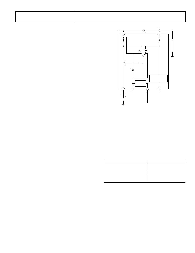
�THEORY� OF� OPERATION�
�NORMAL� OPERATION�
�(7� V� TO� 65� V� SUPPLY� (V+)� RANGE)�
�BATTERY�
�1�
�R1�
�R� SHUNT�
�AD8212�
�I� LOAD�
�8�
�R2�
�In� typical� applications,� the� AD8212� measures� a� small�
�differential� input� voltage� generated� by� a� load� current�
�flowing� through� a� shunt� resistor.�
�The� operational� amplifier� (A1)� is� connected� across� the� shunt�
�resistor� (R� SHUNT� )� with� its� inverting� input� connected� to� the�
�battery/supply� side,� and� the� noninverting� input� connected�
�to� the� load� side� of� the� system.� Amplifier� A1� is� powered� via�
�an� internal� series� regulator� (depicted� as� a� Zener� diode� in�
�Q1�
�A1�
�Figure� 22).� This� regulator� maintains� a� constant� 5� V� between�
�the� battery/supply� terminal� of� the� AD8212� and� COM� (Pin� 2),�
�which� represents� the� lowest� common� point� of� the� internal�
�BIAS�
�CIRCUIT�
�OUTPUT�
�CURRENT�
�COMPENSATION�
�circuitry.�
�A� load� current� flowing� through� the� external� shunt� resistor�
�produces� a� voltage� at� the� input� terminals� of� the� AD8212.�
�Amplifier� A1� responds� by� causing� Transistor� Q1� to� conduct� the�
�VOUT�
�R� OUT�
�5�
�I� OUT�
�2�
�3�
�6�
�necessary� current� through� Resistor� R1� to� equalize� the� potential�
�at� both� the� inverting� and� noninverting� inputs� of� Amplifier� A1.�
�The� current� through� the� emitter� of� Transistor� Q1� (I� OUT� )� is�
�proportional� to� the� input� voltage� (V� SENSE� ),� and,� therefore,� the�
�load� current� (I� LOAD� )� through� the� shunt� resistor� (R� SHUNT� ).� The�
�output� current� (I� OUT� )� is� converted� to� a� voltage� by� using� an�
�external� resistor,� the� value� of� which� is� dependent� on� the� input�
�to� output� gain� equation� desired� in� the� application.�
�The� transfer� function� for� the� AD8212� is�
�I� OUT� =� (� g� m� � V� SENSE� )�
�V� SENSE� =� I� LOAD� � R� SHUNT�
�V� OUT� =� I� OUT� � R� OUT�
�Figure� 22.� Typical� Connection� (7� V� to� 65� V� Supply� (Pin� V+)� Range)�
�When� using� the� AD8212� as� described,� the� battery/supply�
�voltage� in� the� system� must� be� between� 7� V� to� 65� V.� The� 7� V�
�minimum� supply� range� is� necessary� to� turn� on� the� internal�
�regulator� (shown� as� a� Zener� diode� in� Figure� 22).� This� regulated�
�voltage� then� remains� a� constant� 5� V,� regardless� of� the� supply�
�(V+)� voltage.� The� 65� V� maximum� limit� in� this� mode� of�
�operation� is� due� to� the� breakdown� voltage� limitation� of� the�
�AD8212� process.�
�Typically,� a� 1%� resistor� can� be� used� to� convert� the� output�
�current� to� a� voltage.� Table� 4� provides� suggested� R� OUT� values.�
�V� OUT� =� (V� SENSE� � R� OUT� )/� 1000�
�where:�
�g� m� =� 1000� μ� A/V.�
�In� normal� voltage� operation� mode,� the� bias� circuit� is� connected�
�to� GND,� as� shown� in� Figure� 22.� In� this� mode,� I� BIAS� is� typically�
�185� μA� throughout� the� 7� V� to� 65� V� (V+)� range.�
�Table� 4.� Suggested� R� OUT� Values�
�Gain� (V/V)�
�1�
�10�
�20�
�50�
�100�
�R� OUT� (kΩ)�
�1�
�10�
�20�
�49.9�
�100�
�Rev.� B� |� Page� 9� of� 16�
�相关PDF资料 |
PDF描述 |
|---|---|
| AISC-1008-R039G-T | INDUCTOR 39NH 1000MA 2% SMD |
| LT3092ITS8#TRPBF | IC PROG CURRENT SOURCE TSOT23-8 |
| C0603C0G1H430J | CAP CER 43PF 50V 5% NP0 0201 |
| TL431ACLPRAG | IC VREF SHUNT PREC ADJ TO-92-3 |
| C0603C0G1H0R5C | CAP CER 0.5PF 50V NP0 0201 |
相关代理商/技术参数 |
参数描述 |
|---|---|
| AD8212WYRMZ-R71 | 制造商:AD 制造商全称:Analog Devices 功能描述:High Voltage Current Shunt Monitor |
| AD8212WYRMZ-RL | 功能描述:IC CURRENT MONITOR 8MSOP RoHS:是 类别:集成电路 (IC) >> PMIC - 稳流/电流管理 系列:- 产品培训模块:Lead (SnPb) Finish for COTS Obsolescence Mitigation Program 标准包装:50 系列:- 功能:电流开关 检测方法:- 精确度:±10% 输入电压:1.7 V ~ 5.5 V 电流 - 输出:600mA 工作温度:-40°C ~ 125°C 安装类型:表面贴装 封装/外壳:10-UFQFN 供应商设备封装:10-UTQFN(1.4x1.8) 包装:管件 |
| AD8212WYRMZ-RL1 | 制造商:AD 制造商全称:Analog Devices 功能描述:High Voltage Current Shunt Monitor |
| AD8212YRMZ | 功能描述:IC CURRENT MONITOR 8MSOP RoHS:是 类别:集成电路 (IC) >> PMIC - 稳流/电流管理 系列:- 产品培训模块:Lead (SnPb) Finish for COTS Obsolescence Mitigation Program 标准包装:50 系列:- 功能:电流开关 检测方法:- 精确度:±10% 输入电压:1.7 V ~ 5.5 V 电流 - 输出:600mA 工作温度:-40°C ~ 125°C 安装类型:表面贴装 封装/外壳:10-UFQFN 供应商设备封装:10-UTQFN(1.4x1.8) 包装:管件 |
| AD8212YRMZ | 制造商:Analog Devices 功能描述:IC - Current Shunt Monitor 制造商:Analog Devices 功能描述:IC, CURRENT SHUNT MONITOR, 1MHZ, MSOP-8 |
发布紧急采购,3分钟左右您将得到回复。