- 您现在的位置:买卖IC网 > PDF目录22244 > AD8212YRMZ-RL (Analog Devices Inc)IC CURRENT MONITOR 8MSOP PDF资料下载
参数资料
| 型号: | AD8212YRMZ-RL |
| 厂商: | Analog Devices Inc |
| 文件页数: | 10/16页 |
| 文件大小: | 0K |
| 描述: | IC CURRENT MONITOR 8MSOP |
| 标准包装: | 3,000 |
| 功能: | 电流监控器 |
| 检测方法: | 高端 |
| 输入电压: | 7 V ~ 65 V |
| 电流 - 输出: | 500µA |
| 工作温度: | -40°C ~ 125°C |
| 安装类型: | 表面贴装 |
| 封装/外壳: | 8-TSSOP,8-MSOP(0.118",3.00mm 宽) |
| 供应商设备封装: | 8-MSOP |
| 包装: | 带卷 (TR) |
��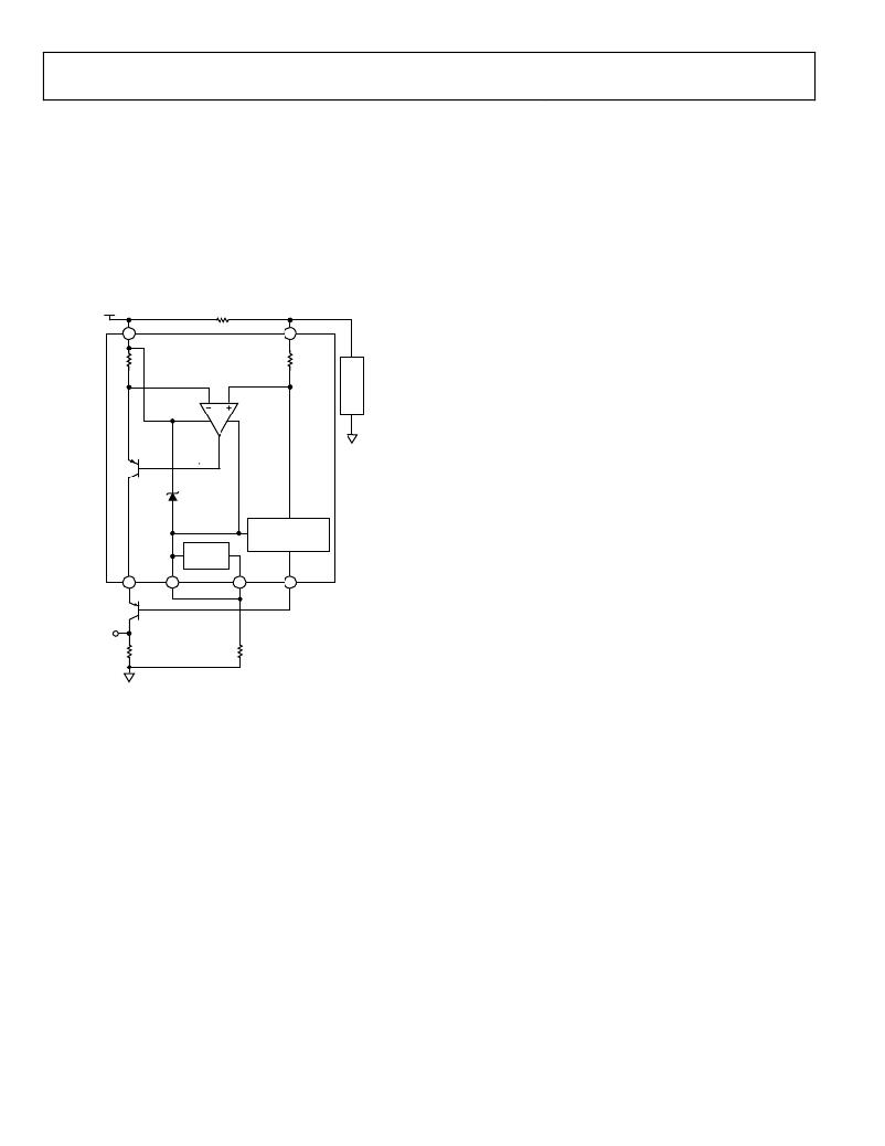 �
�
�AD8212�
�R� SHUNT�
�HIGH� VOLTAGE� OPERATION� USING� AN� EXTERNAL�
�PNP� TRANSISTOR�
�The� AD8212� offers� features� that� simplify� measuring� current� in�
�the� presence� of� common-mode� voltages� greater� than� 65� V.� This�
�is� achieved� by� connecting� an� external� PNP� transistor� at� the�
�output� of� the� AD8212,� as� shown� in� Figure� 23.� The� V� CE� break-�
�down� voltage� of� this� PNP� becomes� the� operating� common-mode�
�range� of� the� AD8212.� PNP� transistors� with� breakdown� voltages�
�exceeding� 300� V� are� inexpensive� and� readily� available� in� small�
�packages.�
�BATTERY�
�In� this� mode� of� operation,� the� supply� current� (I� BIAS� )� of� the�
�AD8212� circuit� increases� based� on� the� supply� range� and� the�
�R� BIAS� resistor� chosen.� For� example�
�if�
�V+� =� 500� V� and� R� BIAS� =� 500� k�
�I� BIAS� =� (� V+� ?� 5� V)/� R� BIAS�
�then,�
�I� BIAS� =� (500� –� 5)/500� kΩ� =� 990� μA�
�In� high� voltage� operation,� it� is� recommended� that� I� BIAS� remain�
�within� 200� μA� to� 1� mA.� This� ensures� that� the� bias� circuit� is�
�1�
�8�
�turned� on,� allowing� the� device� to� function� as� expected.� At� the�
�R1�
�AD8212�
�R2�
�same� time,� the� current� through� the� bias� circuit/regulator� is�
�limited� to� 1� mA.� Refer� to� Figure� 19� and� Figure� 21� for� I� BIAS� and�
�V+� information� when� using� the� AD8212� in� a� high� voltage�
�configuration.�
�A1�
��Transistor� Q2� can� be� a� FET� or� a� bipolar� PNP� transistor.� The�
�Q1�
�latter� is� much� less� expensive,� however� the� magnitude� of� I� OUT�
�conducted� to� the� output� resistor� (R� OUT� )� is� reduced� by� the�
�amount� of� current� lost� through� the� base� of� the� PNP.� This� leads�
�to� an� error� in� the� output� voltage� reading.�
�BIAS�
�CIRCUIT�
�OUTPUT�
�CURRENT�
�COMPENSATION�
�The� AD8212� includes� an� integrated� patented� circuit,� which�
�compensates� for� the� output� current� that� is� lost� through� the� base�
�5�
�2�
�3�
�6�
�of� the� external� PNP� transistor.� This� ensures� that� the� correct�
�transconductance� of� the� amplifier� is� maintained.� The� user� can�
�VOUT�
�Q2�
�opt� for� an� inexpensive� bipolar� PNP,� instead� of� a� FET,� while�
�maintaining� a� comparable� level� of� accuracy.�
�R� OUT�
�R� BIAS�
�OUTPUT� CURRENT� COMPENSATION� CIRCUIT�
�The� base� of� the� external� PNP,� Q2,� is� connected� to� ALPHA�
�Figure� 23.� High� Voltage� Operation� Using� External� PNP�
�The� AD8212� features� an� integrated� 5� V� series� regulator.� This�
�regulator� ensures� that� at� all� times� COM� (Pin� 2),� which� is� the�
�most� negative� of� all� the� terminals,� is� always� 5� V� less� than� the�
�supply� voltage� (V+).� Assuming� a� battery� voltage� (V+)� of� 100� V,�
�it� follows� that� the� voltage� at� COM� (Pin� 2)� is�
�(� V� +)� –� 5� V� =� 95� V�
�The� base� emitter� junction� of� Transistor� Q2,� in� addition� to� the�
�V� be� of� one� internal� transistor,� makes� the� collector� of� Transistor� Q1�
�approximately� equal� to�
�95� V� +� 2(� V� be(Q2)� )� =� 95� V� +� 1.2� V� =� 96.2� V�
�This� voltage� appears� across� external� Transistor� Q2.� The� voltage�
�across� Transistor� Q1� is�
�100� V� –� 96.2� V� =� 3.8� V�
�In� this� manner,� Transistor� Q2� withstands� 95.6� V� and� the�
�internal� Transistor� Q1� is� only� subjected� to� voltages� well� below�
�its� breakdown� capability.�
�(Pin� 6)� of� the� AD8212.� The� current� flowing� in� this� path� is�
�mirrored� inside� the� current� compensation� circuit.� This�
�current� then� flows� in� Resistor� R2,� which� is� the� same� value�
�as� Resistor� R1.� The� voltage� created� by� this� current� across�
�Resistor� R2,� displaces� the� noninverting� input� of� Amplifier� A1�
�by� the� corresponding� voltage.� Amplifier� A1� responds� by� driving�
�the� base� of� Transistor� Q1� so� as� to� force� a� similar� voltage�
�displacement� across� Resistor� R1,� thereby� increasing� I� OUT� .�
�Because� the� current� generated� by� the� output� compensation�
�circuit� is� equal� to� the� base� current� of� Transistor� Q2,� and� the�
�resulting� displacements� across� Resistor� R1� and� Resistor� R2� result�
�in� equal� currents,� the� increment� of� current� added� to� the� output�
�current� is� equivalent� to� the� base� current� of� Transistor� Q2.�
�Therefore,� the� integrated� output� current� compensation� circuit�
�has� corrected� I� OUT� such� that� no� error� results� from� the� base�
�current� lost� at� Transistor� Q2.�
�This� feature� of� the� AD8212� greatly� improves� I� OUT� accuracy� and�
�allows� the� user� to� choose� an� inexpensive� bipolar� PNP� (with� low�
�beta)� with� which� to� monitor� current� in� the� presence� of� high�
�voltages� (typically� several� hundred� volts).�
�Rev.� B� |� Page� 10� of� 16�
�相关PDF资料 |
PDF描述 |
|---|---|
| LM334Z#TR | IC CURRENT SOURCE TO92-3 |
| LM334S8#TRPBF | IC CURRENT SOURCE 8SOIC |
| LM334S8#TR | IC CURRENT SOURCE 8SOIC |
| LM334Z | IC CURRENT SOURCE TO92-3 |
| LM334S8#PBF | IC CURRENT SOURCE 8SOIC |
相关代理商/技术参数 |
参数描述 |
|---|---|
| AD8212YRMZ-RL1 | 制造商:AD 制造商全称:Analog Devices 功能描述:High Voltage Current Shunt Monitor |
| AD8213 | 制造商:AD 制造商全称:Analog Devices 功能描述:Dual, High Voltage Current Shunt Monitor |
| AD8213WHRMZ | 功能描述:Current Monitor Regulator High/Low-Side 10-MSOP 制造商:analog devices inc. 系列:- 包装:管件 零件状态:有效 功能:电流监控器 感应方法:高/低端 精度:±0.25% 电压 - 输入:-2 V ~ 65 V 电流 - 输出:- 工作温度:-40°C ~ 150°C 安装类型:表面贴装 封装/外壳:10-TFSOP,10-MSOP(0.118",3.00mm 宽) 供应商器件封装:10-MSOP 标准包装:50 |
| AD8213WHRMZ-R7 | 功能描述:Current Monitor Regulator High/Low-Side 10-MSOP 制造商:analog devices inc. 系列:- 包装:带卷(TR) 零件状态:有效 功能:电流监控器 感应方法:高/低端 精度:±0.25% 电压 - 输入:-2 V ~ 65 V 电流 - 输出:- 工作温度:-40°C ~ 150°C 安装类型:表面贴装 封装/外壳:10-TFSOP,10-MSOP(0.118",3.00mm 宽) 供应商器件封装:10-MSOP 标准包装:1,000 |
| AD8213WHRMZ-RL | 功能描述:Current Monitor Regulator High/Low-Side 10-MSOP 制造商:analog devices inc. 系列:- 包装:带卷(TR) 零件状态:有效 功能:电流监控器 感应方法:高/低端 精度:±0.25% 电压 - 输入:-2 V ~ 65 V 电流 - 输出:- 工作温度:-40°C ~ 150°C 安装类型:表面贴装 封装/外壳:10-TFSOP,10-MSOP(0.118",3.00mm 宽) 供应商器件封装:10-MSOP 标准包装:3,000 |
发布紧急采购,3分钟左右您将得到回复。