参数资料
| 型号: | AD8223BR-R7 |
| 厂商: | Analog Devices Inc |
| 文件页数: | 7/20页 |
| 文件大小: | 0K |
| 描述: | IC AMP INST R-R LP 8SOIC |
| 标准包装: | 1,000 |
| 放大器类型: | 仪表 |
| 电路数: | 1 |
| 输出类型: | 满摆幅 |
| 转换速率: | 0.3 V/µs |
| -3db带宽: | 200kHz |
| 电流 - 输入偏压: | 12nA |
| 电压 - 输入偏移: | 100µV |
| 电流 - 电源: | 650µA |
| 电压 - 电源,单路/双路(±): | 3 V ~ 24 V,±2 V ~ 12 V |
| 工作温度: | -40°C ~ 85°C |
| 安装类型: | 表面贴装 |
| 封装/外壳: | 8-SOIC(0.154",3.90mm 宽) |
| 供应商设备封装: | 8-SO |
| 包装: | 带卷 (TR) |
AD8223
Rev. 0 | Page 15 of 20
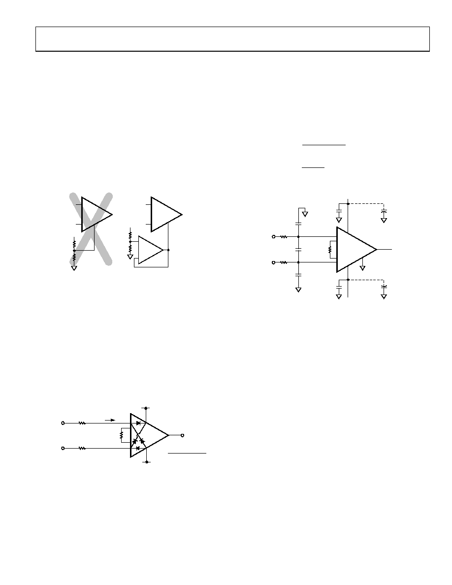
REFERENCE TERMINAL
The output voltage of the AD8223 is developed with respect to
the potential on the reference terminal. This is useful when the
output signal needs to be offset to a precise midsupply level. For
example, a voltage source can be tied to the REF pin to level-
shift the output so that the AD8223 can drive a single-supply
ADC. The REF pin is protected with ESD diodes and should
not exceed either +VS or VS by more than 0.3 V.
For best performance, keep the source impedance to the REF
terminal below 5 Ω. As shown in Figure 31, the reference
terminal, REF, is at one end of a 50 kΩ resistor. Additional
impedance at the REF terminal adds to this resistor and results
in poorer CMRR performance.
INCORRECT
AD8223
VREF
CORRECT
AD8223
OP2177
+
–
VREF
06
92
5-
03
9
Figure 32. Driving the Reference Pin
INPUT PROTECTION
Internal supply referenced clamping diodes allow the input,
reference, output, and gain terminals of the AD8223 to safely
withstand overvoltages of 0.3 V above or below the supplies.
This is true for all gains, and for power-on and power-off. This
last case is particularly important because the signal source and
amplifier can be powered separately.
If the overvoltage is expected to exceed this value, limit the
current through these diodes to about 10 mA using external
current limiting resistors. This is shown in Figure 33. The size
of this resistor is defined by the supply voltage and the required
overvoltage protection.
10mA
1 = 10mA MAX
OUT
AD8223
+
–
VOVER – VS + 0.7V
+VS
–VS
RG
RLIM
RLIM =
VOVER
06
92
5-
04
0
Figure 33. Input Protection
RF INTERFERENCE (RFI)
RF rectification is often a problem when amplifiers are used in
applications where there are strong RF signals. The disturbance
can appear as a small dc offset voltage. High frequency signals
can be filtered with a low-pass, R-C network placed at the input
of the instrumentation amplifier, as shown in Figure 34. The
filter limits the input signal bandwidth according to the follow-
ing relationship:
)
(2
2
1
C
D
Diff
C
R
FilterFreq
C
CM
RC
FilterFreq
2
1
where CD ≥ 10CC.
R
AD8223
+15V
+IN
–IN
0.1F
10F
0.1F
REF
VOUT
–15V
R1
499
CD
47nF
CC
1nF
CC
1nF
4.02k
+
–
+
06
92
5-
04
1
Figure 34. RFI Suppression
Figure 34 shows an example in which the differential filter fre-
quency is approximately 400 Hz, and the common-mode filter
frequency is approximately 40 kHz. The typical dc offset shift
over frequency is less than 1.5 μV, and the RF signal rejection
of the circuit is better than 71 dB.
The resistors were selected to be large enough to isolate the
circuit input from the capacitors but not large enough to
significantly increase the circuit noise. Choose values of R and
CC to minimize RFI. Mismatch between the R × CC at positive
input and the R × CC at negative input degrades the CMRR of
the AD8223. Because of their higher accuracy and stability,
COG/NPO type ceramic capacitors are recommended for the
CC capacitors. The dielectric for the CD capacitor is not as
critical.
相关PDF资料 |
PDF描述 |
|---|---|
| CT0603K25G | VARISTOR 25VRMS 0603 SMD |
| LT1620IS8#TR | IC AMP CURRENT SENSE R-R 8SOIC |
| LT1620CGN#PBF | IC AMP R-R CURRENT SENSE 16-SSOP |
| LT6211CDD#PBF | IC AMP CFA R-R DUAL PROGR 10-DFN |
| AVR-M1608C270KT6AB | VARISTOR 27V 48A 430PF 0603 SMD |
相关代理商/技术参数 |
参数描述 |
|---|---|
| AD8223BR-RL | 功能描述:IC AMP INST R-R LP 8SOIC RoHS:否 类别:集成电路 (IC) >> Linear - Amplifiers - Instrumentation 系列:- 标准包装:50 系列:- 放大器类型:通用 电路数:2 输出类型:满摆幅 转换速率:1.8 V/µs 增益带宽积:6.5MHz -3db带宽:4.5MHz 电流 - 输入偏压:5nA 电压 - 输入偏移:100µV 电流 - 电源:65µA 电流 - 输出 / 通道:35mA 电压 - 电源,单路/双路(±):1.8 V ~ 5.25 V,±0.9 V ~ 2.625 V 工作温度:-40°C ~ 85°C 安装类型:表面贴装 封装/外壳:10-TFSOP,10-MSOP(0.118",3.00mm 宽) 供应商设备封装:10-MSOP 包装:管件 |
| AD8223BRZ | 功能描述:IC AMP INST R-R LP 8SOIC RoHS:是 类别:集成电路 (IC) >> Linear - Amplifiers - Instrumentation 系列:- 产品培训模块:Differential Circuit Design Techniques for Communication Applications 标准包装:1 系列:- 放大器类型:RF/IF 差分 电路数:1 输出类型:差分 转换速率:9800 V/µs 增益带宽积:- -3db带宽:2.9GHz 电流 - 输入偏压:3µA 电压 - 输入偏移:- 电流 - 电源:40mA 电流 - 输出 / 通道:- 电压 - 电源,单路/双路(±):3 V ~ 3.6 V 工作温度:-40°C ~ 85°C 安装类型:表面贴装 封装/外壳:16-VQFN 裸露焊盘,CSP 供应商设备封装:16-LFCSP-VQ 包装:剪切带 (CT) 产品目录页面:551 (CN2011-ZH PDF) 其它名称:ADL5561ACPZ-R7CT |
| AD8223BRZ-R7 | 功能描述:IC AMP INST R-R LP 8SOIC RoHS:是 类别:集成电路 (IC) >> Linear - Amplifiers - Instrumentation 系列:- 标准包装:1,000 系列:- 放大器类型:电压反馈 电路数:4 输出类型:满摆幅 转换速率:33 V/µs 增益带宽积:20MHz -3db带宽:30MHz 电流 - 输入偏压:2nA 电压 - 输入偏移:3000µV 电流 - 电源:2.5mA 电流 - 输出 / 通道:30mA 电压 - 电源,单路/双路(±):4.5 V ~ 16.5 V,±2.25 V ~ 8.25 V 工作温度:-40°C ~ 85°C 安装类型:表面贴装 封装/外壳:14-SOIC(0.154",3.90mm 宽) 供应商设备封装:14-SOIC 包装:带卷 (TR) |
| AD8223BRZ-RL | 功能描述:IC AMP INST R-R LP 8SOIC RoHS:是 类别:集成电路 (IC) >> Linear - Amplifiers - Instrumentation 系列:- 标准包装:1,000 系列:- 放大器类型:电压反馈 电路数:4 输出类型:满摆幅 转换速率:33 V/µs 增益带宽积:20MHz -3db带宽:30MHz 电流 - 输入偏压:2nA 电压 - 输入偏移:3000µV 电流 - 电源:2.5mA 电流 - 输出 / 通道:30mA 电压 - 电源,单路/双路(±):4.5 V ~ 16.5 V,±2.25 V ~ 8.25 V 工作温度:-40°C ~ 85°C 安装类型:表面贴装 封装/外壳:14-SOIC(0.154",3.90mm 宽) 供应商设备封装:14-SOIC 包装:带卷 (TR) |
| AD8224 | 制造商:AD 制造商全称:Analog Devices 功能描述:Wide Supply Range, Micropower, |
发布紧急采购,3分钟左右您将得到回复。