- 您现在的位置:买卖IC网 > PDF目录5789 > AD8224ACPZ-R7 (Analog Devices Inc)IC AMP INST JFET R-R LP 16LFCSP PDF资料下载
参数资料
| 型号: | AD8224ACPZ-R7 |
| 厂商: | Analog Devices Inc |
| 文件页数: | 15/28页 |
| 文件大小: | 0K |
| 描述: | IC AMP INST JFET R-R LP 16LFCSP |
| 产品培训模块: | Instrumentation Amplifiers Performance |
| 标准包装: | 1 |
| 放大器类型: | 仪表 |
| 电路数: | 2 |
| 输出类型: | 满摆幅 |
| 转换速率: | 2 V/µs |
| -3db带宽: | 1.5MHz |
| 电流 - 输入偏压: | 25pA |
| 电压 - 输入偏移: | 300µV |
| 电流 - 电源: | 750µA |
| 电流 - 输出 / 通道: | 15mA |
| 电压 - 电源,单路/双路(±): | 4.5 V ~ 36 V,±2.25 V ~ 18 V |
| 工作温度: | -40°C ~ 85°C |
| 安装类型: | 表面贴装 |
| 封装/外壳: | 16-VQFN 裸露焊盘,CSP |
| 供应商设备封装: | 16-LFCSP-VQ |
| 包装: | 标准包装 |
| 产品目录页面: | 771 (CN2011-ZH PDF) |
| 配用: | AD8224-EVALZ-ND - BOARD EVALUATION AD8224 |
| 其它名称: | AD8224ACPZ-R7DKR |
第1页第2页第3页第4页第5页第6页第7页第8页第9页第10页第11页第12页第13页第14页当前第15页第16页第17页第18页第19页第20页第21页第22页第23页第24页第25页第26页第27页第28页
AD8224
Data Sheet
Rev. C | Page 22 of 28
To preserve maximum pin compatibility with other dual
instrumentation amplifiers, such as the AD8222, leave the pad
unconnected. This can be done by not soldering the paddle at
all or by soldering the part to a landing that is a not connected
to any other net. For high vibration applications, a landing is
recommended.
Because the AD8224 dissipates little power, heat dissipation is
rarely an issue. If improved heat dissipation is desired (for example,
when driving heavy loads), connect the exposed pad to the
positive supply rail. For the best heat dissipation performance,
the positive supply rail should be a plane in the board. See
the Thermal Resistance section for more information.
Common-Mode Rejection over Frequency
The AD8224 has a higher CMRR over frequency than typical
in-amps, which gives it greater immunity to disturbances, such
as line noise and its associated harmonics. A well-implemented
layout is required to maintain this high performance. Input
source impedances should be matched closely. Source resistance
should be placed close to the inputs so that it interacts with as
little parasitic capacitance as possible.
Parasitics at the RGx pins can also affect CMRR over frequency.
The PCB should be laid out so that the parasitic capacitances at
each pin match. Traces from the gain setting resistor to the RGx
pins should be kept short to minimize parasitic inductance.
Reference
Errors introduced at the reference terminal feed directly to
the output. Take care to tie the REFx pins to the appropriate
local ground.
Power Supplies
A stable dc voltage should be used to power the instrumentation
amplifier. Noise on the supply pins can adversely affect
performance.
The AD8224 has two positive supply pins (Pin 5 and Pin 16)
and two negative supply pins (Pin 8 and Pin 13). While the part
functions with only one pin from each supply pair connected,
both pins should be connected for specified performance and
optimum reliability.
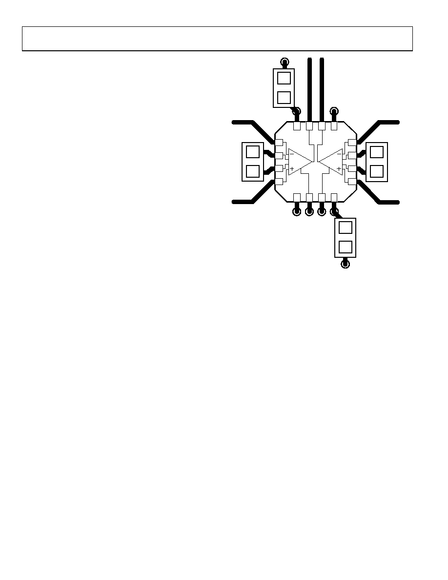
The AD8224 should be decoupled with 0.1 F bypass capacitors,
one for each supply. Place the positive supply decoupling
capacitor near Pin 16, and the negative supply decoupling
capacitor near Pin 8. Each supply should also be decoupled with
a 10 F tantalum capacitor. The tantalum capacitor can be
placed further away from the AD8224 and can generally be
shared by other precision integrated circuits. Figure 58 shows an
example layout.
AD8224
1
2
3
4
12
11
9
5
6
7
8
13
14
15
16
0.1F
RG
10
06286-
059
Figure 58. Example Layout
SOLDER WASH
The solder process can leave flux and other contaminants on
the board. When these contaminants are between the AD8224
leads and thermal pad, they can create leakage paths that are
larger than the AD8224 bias currents. A thorough washing
process removes these contaminants and restores the device’s
excellent bias current performance.
INPUT BIAS CURRENT RETURN PATH
The input bias current of the AD8224 must have a return path
to common. When the source, such as a transformer, cannot
provide a return current path, one should be created, as shown
INPUT PROTECTION
All terminals of the AD8224 are protected against ESD. ESD
protection is guaranteed to 4 kV (human body model). In addition,
the input structure allows for dc overload conditions a diode
drop above the positive supply and a diode drop below the
negative supply. Voltages beyond a diode drop of the supplies
cause the ESD diodes to conduct and enable current to flow
through the diode. Therefore, an external resistor should be
used in series with each of the inputs to limit current for
voltages beyond the supplies. In either scenario, the AD8224
safely handles a continuous 6 mA current at room temperature.
相关PDF资料 |
PDF描述 |
|---|---|
| 0001.2713.11 | FUSE 8A 250V 5X20 T-LAG SMD |
| 0001.2714.11 | FUSE 10A 250V 5X20 T-LAG SMD |
| 326859 | CONN SPADE 10-12 AWG #6 YEL PIDG |
| 77311-101-34LF | BERGSTIK |
| 0001.2715.11 | FUSE 12.5A 250V 5X20 T-LAG SMD |
相关代理商/技术参数 |
参数描述 |
|---|---|
| AD8224ACPZ-RL | 功能描述:IC AMP INST JFET R-R LP 16LFCSP RoHS:是 类别:集成电路 (IC) >> Linear - Amplifiers - Instrumentation 系列:- 标准包装:50 系列:- 放大器类型:J-FET 电路数:2 输出类型:- 转换速率:13 V/µs 增益带宽积:3MHz -3db带宽:- 电流 - 输入偏压:65pA 电压 - 输入偏移:3000µV 电流 - 电源:1.4mA 电流 - 输出 / 通道:- 电压 - 电源,单路/双路(±):7 V ~ 36 V,±3.5 V ~ 18 V 工作温度:-40°C ~ 85°C 安装类型:通孔 封装/外壳:8-DIP(0.300",7.62mm) 供应商设备封装:8-PDIP 包装:管件 |
| AD8224ACPZ-WP | 功能描述:IC AMP INST JFET R-R LP 16LFCSP RoHS:是 类别:集成电路 (IC) >> Linear - Amplifiers - Instrumentation 系列:- 标准包装:1 系列:- 放大器类型:通用 电路数:4 输出类型:满摆幅 转换速率:0.028 V/µs 增益带宽积:105kHz -3db带宽:- 电流 - 输入偏压:3nA 电压 - 输入偏移:100µV 电流 - 电源:3.3µA 电流 - 输出 / 通道:12mA 电压 - 电源,单路/双路(±):2.7 V ~ 12 V,±1.35 V ~ 6 V 工作温度:-40°C ~ 85°C 安装类型:表面贴装 封装/外壳:14-TSSOP(0.173",4.40mm 宽) 供应商设备封装:14-TSSOP 包装:剪切带 (CT) 其它名称:OP481GRUZ-REELCT |
| AD8224BCPZ-R7 | 功能描述:IC AMP INST JFET R-R LP 16LFCSP RoHS:是 类别:集成电路 (IC) >> Linear - Amplifiers - Instrumentation 系列:- 标准包装:100 系列:- 放大器类型:通用 电路数:1 输出类型:- 转换速率:0.2 V/µs 增益带宽积:- -3db带宽:- 电流 - 输入偏压:100pA 电压 - 输入偏移:30µV 电流 - 电源:380µA 电流 - 输出 / 通道:- 电压 - 电源,单路/双路(±):±2 V ~ 18 V 工作温度:0°C ~ 70°C 安装类型:表面贴装 封装/外壳:8-SOIC(0.154",3.90mm 宽) 供应商设备封装:8-SO 包装:管件 |
| AD8224BCPZ-RL | 功能描述:IC AMP INST JFET R-R LP 16LFCSP RoHS:是 类别:集成电路 (IC) >> Linear - Amplifiers - Instrumentation 系列:- 标准包装:2,500 系列:Excalibur™ 放大器类型:J-FET 电路数:1 输出类型:- 转换速率:45 V/µs 增益带宽积:10MHz -3db带宽:- 电流 - 输入偏压:20pA 电压 - 输入偏移:490µV 电流 - 电源:1.7mA 电流 - 输出 / 通道:48mA 电压 - 电源,单路/双路(±):4.5 V ~ 38 V,±2.25 V ~ 19 V 工作温度:-40°C ~ 85°C 安装类型:表面贴装 封装/外壳:8-SOIC(0.154",3.90mm 宽) 供应商设备封装:8-SOIC 包装:带卷 (TR) |
| AD8224BCPZ-WP | 功能描述:IC AMP INST JFET R-R LP 16LFCSP RoHS:是 类别:集成电路 (IC) >> Linear - Amplifiers - Instrumentation 系列:- 标准包装:2,500 系列:Excalibur™ 放大器类型:J-FET 电路数:1 输出类型:- 转换速率:45 V/µs 增益带宽积:10MHz -3db带宽:- 电流 - 输入偏压:20pA 电压 - 输入偏移:490µV 电流 - 电源:1.7mA 电流 - 输出 / 通道:48mA 电压 - 电源,单路/双路(±):4.5 V ~ 38 V,±2.25 V ~ 19 V 工作温度:-40°C ~ 85°C 安装类型:表面贴装 封装/外壳:8-SOIC(0.154",3.90mm 宽) 供应商设备封装:8-SOIC 包装:带卷 (TR) |
发布紧急采购,3分钟左右您将得到回复。