参数资料
| 型号: | AD8226ARMZ |
| 厂商: | Analog Devices Inc |
| 文件页数: | 13/28页 |
| 文件大小: | 0K |
| 描述: | IC AMP INST R-R LP 13MA 8MSOP |
| 标准包装: | 50 |
| 放大器类型: | 仪表 |
| 电路数: | 1 |
| 输出类型: | 满摆幅 |
| 转换速率: | 0.6 V/µs |
| -3db带宽: | 1.5MHz |
| 电流 - 输入偏压: | 20nA |
| 电压 - 输入偏移: | 200µV |
| 电流 - 电源: | 350µA |
| 电流 - 输出 / 通道: | 13mA |
| 电压 - 电源,单路/双路(±): | 2.2 V ~ 36 V,±1.35 V ~ 18 V |
| 工作温度: | -40°C ~ 125°C |
| 安装类型: | 表面贴装 |
| 封装/外壳: | 8-TSSOP,8-MSOP(0.118",3.00mm 宽) |
| 供应商设备封装: | 8-MSOP |
| 包装: | 管件 |
第1页第2页第3页第4页第5页第6页第7页第8页第9页第10页第11页第12页当前第13页第14页第15页第16页第17页第18页第19页第20页第21页第22页第23页第24页第25页第26页第27页第28页
AD8226
Data Sheet
Rev. C | Page 20 of 28
REFERENCE TERMINAL
The output voltage of the AD8226 is developed with respect to
the potential on the reference terminal. This is useful when the
output signal needs to be offset to a precise midsupply level. For
example, a voltage source can be tied to the REF pin to level-
shift the output so that the AD8226 can drive a single-supply
ADC. The REF pin is protected with ESD diodes and should
not exceed either +VS or VS by more than 0.3 V.
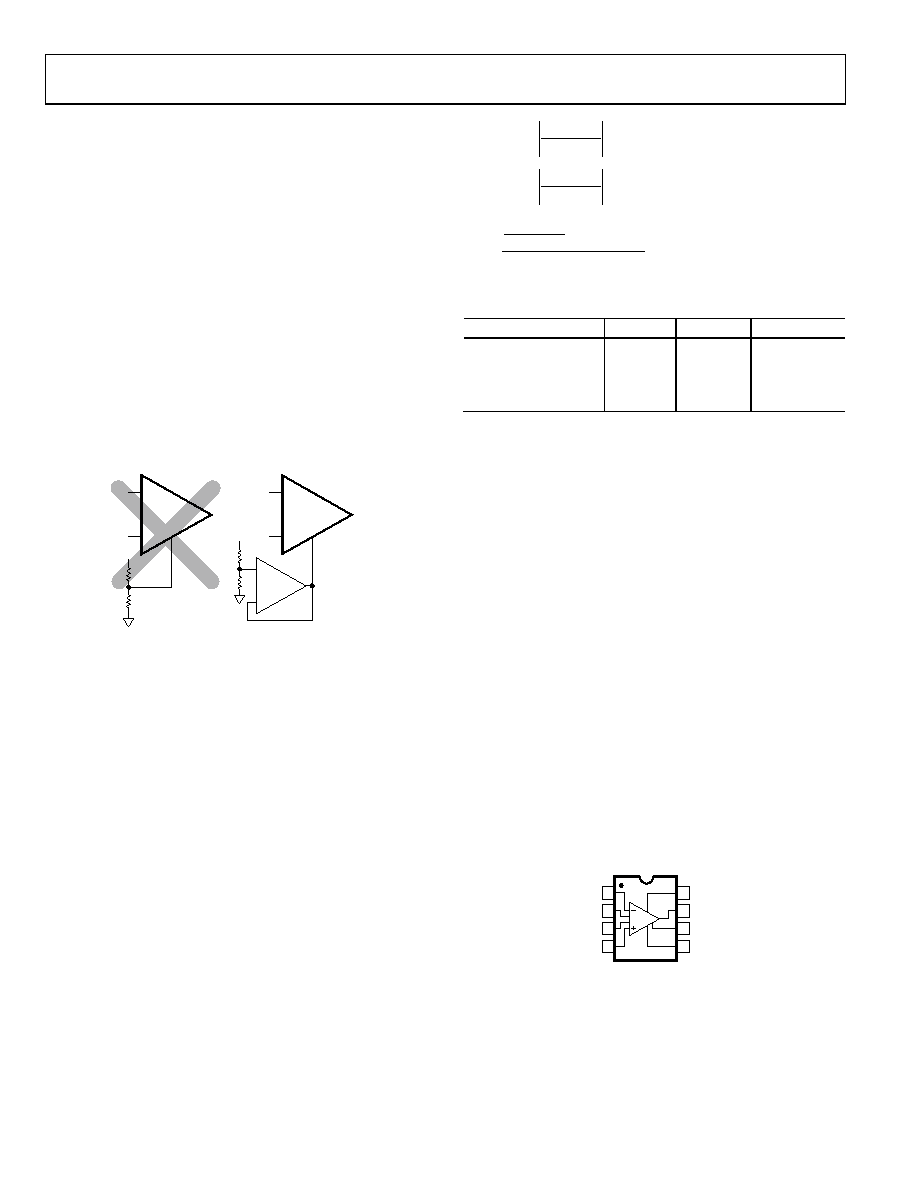
For the best performance, source impedance to the REF
terminal should be kept below 2 . As shown in Figure 58,
the reference terminal, REF, is at one end of a 50 kΩ resistor.
Additional impedance at the REF terminal adds to this 50 kΩ
resistor and results in amplification of the signal connected to
the positive input. The amplification from the additional RREF
can be computed by 2(50 kΩ + RREF)/(100 kΩ + RREF).
Only the positive signal path is amplified; the negative path
is unaffected. This uneven amplification degrades CMRR.
INCORRECT
V
CORRECT
AD8226
OP1177
+
–
V
07036-
004
REF
AD8226
REF
Figure 59. Driving the Reference Pin
INPUT VOLTAGE RANGE
Figure 9 through Figure 15 and Figure 18 show the allowable
common-mode input voltage ranges for various output voltages
and supply voltages. The 3-op-amp architecture of the AD8226
applies gain in the first stage before removing common-mode
voltage with the difference amplifier stage. Internal nodes between
the first and second stages (Node 1 and Node 2 in Figure 58)
experience a combination of a gained signal, a common-mode
signal, and a diode drop. This combined signal can be limited
by the voltage supplies even when the individual input and
output signals are not limited.
For most applications, Figure 9 through Figure 15 and Figure 18
provide sufficient information to achieve a good design. For
applications where a more detailed understanding is needed,
Equation 1 to Equation 3 can be used to understand how the
gain (G), common-mode input voltage (VCM), differential input
voltage (VDIFF), and reference voltage (VREF) interact. The values for
These three formulas, along with the input and output range
specifications in Table 2 and Table 3, set the operating boundaries
of the part.
LIMIT
S
DIFF
CM
V
G
V
+
>
2
)
)(
(
(1)
LIMIT
S
DIFF
CM
V
G
V
+
+
<
+
2
)
)(
(
(2)
LIMIT
REF
S
REF
CM
DIFF
V
G
V
_
2
)
)(
(
+
<
+
(3)
Table 8. Input Voltage Range Constants for Various
Temperatures
Temperature
V
LIMIT
V
+LIMIT
V
REF_LIMIT
40°C
0.55 V
0.8 V
1.3 V
+25°C
0.35 V
0.7 V
1.15 V
+85°C
0.15 V
0.65 V
1.05 V
+125°C
0.05 V
0.6 V
0.9 V
Performance Across Temperature
The common-mode input range shifts upward with temper-
ature. At cold temperatures, the part requires extra headroom
from the positive supply, and operation near the negative supply
has more margin. Conversely, hot temperatures require less
headroom from the positive supply, but are the worst-case
conditions for input voltages near the negative supply.
Recommendation for Best Performance
A typical part functions up to the boundaries described in this
section. However, for best performance, designing with a few
hundred millivolts extra margin is recommended. As signals
approach the boundary, internal transistors begin to saturate,
which can affect frequency and linearity performance.
If the application requirements exceed the boundaries, one
solution is to apply less gain with the AD8226, and then apply
additional gain later in the signal chain. Another option is to
use the pin-compatible AD8227.
LAYOUT
To ensure optimum performance of the AD8226 at the PCB
level, care must be taken in the design of the board layout.
The AD8226 pins are arranged in a logical manner to aid in
this task.
8
7
6
5
1
2
3
4
–IN
RG
+VS
VOUT
REF
–VS
+IN
TOP VIEW
(Not to Scale)
AD8226
07036-
005
Figure 60. Pinout Diagram
相关PDF资料 |
PDF描述 |
|---|---|
| 3404.2416.22 | FUSE&HOLDER 1A 125V FAST SMD |
| AD8671ARMZ | IC OPAMP GP 10MHZ PREC LN 8MSOP |
| TA35-C2F3F200C0 | CIRCUIT BRKR THERMAL 20A RED |
| 3404.2415.22 | FUSE&HOLDER 800MA 125V FAST SMD |
| 0713085458 | CONN HEADER BKWY SMD TIN 58POS |
相关代理商/技术参数 |
参数描述 |
|---|---|
| AD8226ARMZ-R7 | 功能描述:IC AMP INST R-R LP 13MA 8MSOP RoHS:是 类别:集成电路 (IC) >> Linear - Amplifiers - Instrumentation 系列:- 产品培训模块:Differential Circuit Design Techniques for Communication Applications 标准包装:1 系列:- 放大器类型:RF/IF 差分 电路数:1 输出类型:差分 转换速率:9800 V/µs 增益带宽积:- -3db带宽:2.9GHz 电流 - 输入偏压:3µA 电压 - 输入偏移:- 电流 - 电源:40mA 电流 - 输出 / 通道:- 电压 - 电源,单路/双路(±):3 V ~ 3.6 V 工作温度:-40°C ~ 85°C 安装类型:表面贴装 封装/外壳:16-VQFN 裸露焊盘,CSP 供应商设备封装:16-LFCSP-VQ 包装:剪切带 (CT) 产品目录页面:551 (CN2011-ZH PDF) 其它名称:ADL5561ACPZ-R7CT |
| AD8226ARMZ-RL | 功能描述:IC AMP INST R-R LP 13MA 8MSOP RoHS:是 类别:集成电路 (IC) >> Linear - Amplifiers - Instrumentation 系列:- 标准包装:2,500 系列:- 放大器类型:通用 电路数:1 输出类型:满摆幅 转换速率:0.11 V/µs 增益带宽积:350kHz -3db带宽:- 电流 - 输入偏压:4nA 电压 - 输入偏移:20µV 电流 - 电源:260µA 电流 - 输出 / 通道:20mA 电压 - 电源,单路/双路(±):2.7 V ~ 36 V,±1.35 V ~ 18 V 工作温度:-40°C ~ 85°C 安装类型:表面贴装 封装/外壳:8-SOIC(0.154",3.90mm 宽) 供应商设备封装:8-SO 包装:带卷 (TR) |
| AD8226ARZ | 功能描述:IC AMP INST R-R LP 13MA 8SOIC RoHS:是 类别:集成电路 (IC) >> Linear - Amplifiers - Instrumentation 系列:- 其它有关文件:Automotive Product Guide 产品培训模块:Lead (SnPb) Finish for COTS Obsolescence Mitigation Program 标准包装:1 系列:- 放大器类型:通用 电路数:1 输出类型:满摆幅 转换速率:3 V/µs 增益带宽积:10MHz -3db带宽:- 电流 - 输入偏压:1pA 电压 - 输入偏移:70µV 电流 - 电源:2.5mA 电流 - 输出 / 通道:48mA 电压 - 电源,单路/双路(±):2.7 V ~ 5.5 V,±1.35 V ~ 2.75 V 工作温度:-40°C ~ 125°C 安装类型:表面贴装 封装/外壳:SOT-23-6 供应商设备封装:SOT-6 包装:Digi-Reel® 其它名称:MAX4475AUT#TG16DKR |
| AD8226ARZ-R7 | 功能描述:IC AMP INST R-R LP 13MA 8SOIC RoHS:是 类别:集成电路 (IC) >> Linear - Amplifiers - Instrumentation 系列:- 产品培训模块:Differential Circuit Design Techniques for Communication Applications 标准包装:1 系列:- 放大器类型:RF/IF 差分 电路数:1 输出类型:差分 转换速率:9800 V/µs 增益带宽积:- -3db带宽:2.9GHz 电流 - 输入偏压:3µA 电压 - 输入偏移:- 电流 - 电源:40mA 电流 - 输出 / 通道:- 电压 - 电源,单路/双路(±):3 V ~ 3.6 V 工作温度:-40°C ~ 85°C 安装类型:表面贴装 封装/外壳:16-VQFN 裸露焊盘,CSP 供应商设备封装:16-LFCSP-VQ 包装:剪切带 (CT) 产品目录页面:551 (CN2011-ZH PDF) 其它名称:ADL5561ACPZ-R7CT |
| AD8226ARZ-RL | 功能描述:IC AMP INST R-R LP 13MA 8SOIC RoHS:是 类别:集成电路 (IC) >> Linear - Amplifiers - Instrumentation 系列:- 标准包装:2,500 系列:- 放大器类型:通用 电路数:1 输出类型:满摆幅 转换速率:0.11 V/µs 增益带宽积:350kHz -3db带宽:- 电流 - 输入偏压:4nA 电压 - 输入偏移:20µV 电流 - 电源:260µA 电流 - 输出 / 通道:20mA 电压 - 电源,单路/双路(±):2.7 V ~ 36 V,±1.35 V ~ 18 V 工作温度:-40°C ~ 85°C 安装类型:表面贴装 封装/外壳:8-SOIC(0.154",3.90mm 宽) 供应商设备封装:8-SO 包装:带卷 (TR) |
发布紧急采购,3分钟左右您将得到回复。