参数资料
| 型号: | AD822ARMZ |
| 厂商: | Analog Devices Inc |
| 文件页数: | 10/24页 |
| 文件大小: | 0K |
| 描述: | IC OPAMP GP R-R 1.9MHZ LP 8MSOP |
| 设计资源: | 16-Bit Fully Isolated 4 mA to 20 mA Output Module Using AD5662, ADuM1401, and External Amplifiers (CN0064) |
| 标准包装: | 50 |
| 放大器类型: | 通用 |
| 电路数: | 2 |
| 输出类型: | 满摆幅 |
| 转换速率: | 3 V/µs |
| 增益带宽积: | 1.9MHz |
| -3db带宽: | 1.9MHz |
| 电流 - 输入偏压: | 2pA |
| 电压 - 输入偏移: | 400µV |
| 电流 - 电源: | 1.4mA |
| 电流 - 输出 / 通道: | 20mA |
| 电压 - 电源,单路/双路(±): | 3 V ~ 36 V,±1.5 V ~ 18 V |
| 工作温度: | -40°C ~ 85°C |
| 安装类型: | 表面贴装 |
| 封装/外壳: | 8-TSSOP,8-MSOP(0.118",3.00mm 宽) |
| 供应商设备封装: | 8-MSOP |
| 包装: | 管件 |
AD822
Rev. I | Page 18 of 24
APPLICATIONS INFORMATION
INPUT CHARACTERISTICS
In the AD822, N-channel JFETs are used to provide a low offset,
low noise, high impedance input stage. Minimum input common-
mode voltage extends from 0.2 V below VS to 1 V less than +VS.
Driving the input voltage closer to the positive rail causes a loss
of amplifier bandwidth (as can be seen by comparing the large
signal responses shown in Figure 34 and Figure 37) and increased
common-mode voltage error as illustrated in Figure 20.
The AD822 does not exhibit phase reversal for input voltages
up to and including +VS. Figure 42 shows the response of an
AD822 voltage follower to a 0 V to 5 V (+VS) square wave input.
The input and output are superimposed. The output tracks the
input up to +VS without phase reversal. The reduced bandwidth
above a 4 V input causes the rounding of the output waveform.
For input voltages greater than +VS, a resistor in series with the
AD822 noninverting input prevents phase reversal, at the expense
of greater input voltage noise. This is illustrated in Figure 42.
Because the input stage uses N-channel JFETs, input current
during normal operation is negative; the current flows out from
the input terminals. If the input voltage is driven more positive
than +VS 0.4 V, then the input current reverses direction as
internal device junctions become forward biased. This is illu-
strated in Figure 7.
A current limiting resistor should be used in series with the input
of the AD822 if there is a possibility of the input voltage exceed-
ing the positive supply by more than 300 mV, or if an input voltage
is applied to the AD822 when +VS or VS = 0 V. The amplifier is
damaged if left in that condition for more than 10 seconds. A 1 kΩ
resistor allows the amplifier to withstand up to 10 V of conti-
nuous overvoltage and increases the input voltage noise by a
negligible amount.
Input voltages less than VS are a completely different story. The
amplifier can safely withstand input voltages 20 V below the
negative supply voltage if the total voltage from the positive
supply to the input terminal is less than 36 V. In addition, the
input stage typically maintains picoampere (pA) level input
currents across that input voltage range.
The AD822 is designed for 13 nV/√Hz wideband input voltage
noise and maintains low noise performance to low frequencies
(refer to Figure 14). This noise performance, along with the
AD822 low input current and current noise, means that the
AD822 contributes negligible noise for applications with source
resistances greater than 10 kΩ and signal bandwidths greater
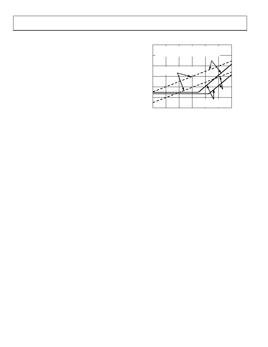
than 1 kHz. This is illustrated in Figure 43.
100k
0.1
10k
1k
100
10
1
WHENEVER JOHNSON NOISE IS GREATER THAN
AMPLIFIER NOISE, AMPLIFIER NOISE CAN BE
CONSIDERED NEGLIGIBLE FOR APPLICATION.
1kHz
AMPLIFIER-GENERATED
NOISE
10Hz
10k
100k
1M
10M
100M
1G
10G
SOURCE IMPEDANCE (
)
IN
PU
T
VO
L
T
A
G
E
N
O
IS
E
(
V)
RESISTOR JOHNSON
NOISE
00
87
4-
0
43
Figure 43. Total Noise vs. Source Impedance
OUTPUT CHARACTERISTICS
The AD822 unique bipolar rail-to-rail output stage swings within
5 mV of the negative supply and 10 mV of the positive supply with
no external resistive load. The approximate output saturation
resistance of the AD822 is 40 Ω sourcing and 20 Ω sinking, which
can be used to estimate output saturation voltage when driving
heavier current loads. For instance, when sourcing 5 mA, the
saturation voltage to the positive supply rail is 200 mV; when
sinking 5 mA, the saturation voltage to the negative rail is 100 mV.
The open-loop gain characteristic of the amplifier changes as a
function of resistive load, as shown in Figure 10 to Figure 13.
For load resistances over 20 kΩ, the AD822 input error voltage
is virtually unchanged until the output voltage is driven to 180 mV
of either supply.
If the AD822 output is overdriven so that either of the output
devices are saturated, the amplifier recovers within 2 μs of its
input returning to the linear operating region of the amplifier.
Direct capacitive loads interact with the effective output imped-
ance of the amplifier to form an additional pole in the amplifier
feedback loop, which can cause excessive peaking on the pulse
response or loss of stability. The worst case occurs when the
amplifier is used as a unity-gain follower. Figure 44 shows the
AD822 pulse response as a unity-gain follower driving 350 pF.
This amount of overshoot indicates approximately 20° of phase
margin—the system is stable, but nearing the edge. Configurations
with less loop gain, and as a result less loop bandwidth, are
much less sensitive to capacitance load effects.
相关PDF资料 |
PDF描述 |
|---|---|
| AD744JR | IC OPAMP BIFET 13MHZ PREC 8SOIC |
| 0001.2712.11 | FUSE 6.3A 250V 5X20 T-LAG SMD |
| 2026-40-CB | GAS DISCHARGE TUBE 3 POLE |
| AD8224ACPZ-R7 | IC AMP INST JFET R-R LP 16LFCSP |
| 0001.2713.11 | FUSE 8A 250V 5X20 T-LAG SMD |
相关代理商/技术参数 |
参数描述 |
|---|---|
| AD822ARMZ | 制造商:Analog Devices 功能描述:IC OP-AMP 1.8MHz 3V/ MSOP-8 |
| AD822ARMZ-R2 | 功能描述:IC OPAMP GP R-R 1.9MHZ LP 8MSOP RoHS:是 类别:集成电路 (IC) >> Linear - Amplifiers - Instrumentation 系列:- 标准包装:2,500 系列:- 放大器类型:通用 电路数:1 输出类型:满摆幅 转换速率:0.11 V/µs 增益带宽积:350kHz -3db带宽:- 电流 - 输入偏压:4nA 电压 - 输入偏移:20µV 电流 - 电源:260µA 电流 - 输出 / 通道:20mA 电压 - 电源,单路/双路(±):2.7 V ~ 36 V,±1.35 V ~ 18 V 工作温度:-40°C ~ 85°C 安装类型:表面贴装 封装/外壳:8-SOIC(0.154",3.90mm 宽) 供应商设备封装:8-SO 包装:带卷 (TR) |
| AD822ARMZ-R2 | 制造商:Analog Devices 功能描述:INST AMP PRECISION DUAL 8MSOP |
| AD822ARMZ-REEL | 功能描述:IC OPAMP GP R-R 1.9MHZ LP 8MSOP RoHS:是 类别:集成电路 (IC) >> Linear - Amplifiers - Instrumentation 系列:- 产品培训模块:Differential Circuit Design Techniques for Communication Applications 标准包装:1 系列:- 放大器类型:RF/IF 差分 电路数:1 输出类型:差分 转换速率:9800 V/µs 增益带宽积:- -3db带宽:2.9GHz 电流 - 输入偏压:3µA 电压 - 输入偏移:- 电流 - 电源:40mA 电流 - 输出 / 通道:- 电压 - 电源,单路/双路(±):3 V ~ 3.6 V 工作温度:-40°C ~ 85°C 安装类型:表面贴装 封装/外壳:16-VQFN 裸露焊盘,CSP 供应商设备封装:16-LFCSP-VQ 包装:剪切带 (CT) 产品目录页面:551 (CN2011-ZH PDF) 其它名称:ADL5561ACPZ-R7CT |
| AD822AR-REEL | 功能描述:IC OPAMP GP R-R 1.9MHZ LP 8SOIC RoHS:否 类别:集成电路 (IC) >> Linear - Amplifiers - Instrumentation 系列:- 标准包装:1 系列:- 放大器类型:通用 电路数:4 输出类型:满摆幅 转换速率:0.028 V/µs 增益带宽积:105kHz -3db带宽:- 电流 - 输入偏压:3nA 电压 - 输入偏移:100µV 电流 - 电源:3.3µA 电流 - 输出 / 通道:12mA 电压 - 电源,单路/双路(±):2.7 V ~ 12 V,±1.35 V ~ 6 V 工作温度:-40°C ~ 85°C 安装类型:表面贴装 封装/外壳:14-TSSOP(0.173",4.40mm 宽) 供应商设备封装:14-TSSOP 包装:剪切带 (CT) 其它名称:OP481GRUZ-REELCT |
发布紧急采购,3分钟左右您将得到回复。