- 您现在的位置:买卖IC网 > PDF目录373941 > AD824AR-14-3V (ANALOG DEVICES INC) VARISTOR 14V RMS 14MM RADIAL PDF资料下载
参数资料
| 型号: | AD824AR-14-3V |
| 厂商: | ANALOG DEVICES INC |
| 元件分类: | 运动控制电子 |
| 英文描述: | VARISTOR 14V RMS 14MM RADIAL |
| 中文描述: | QUAD OP-AMP, 4000 uV OFFSET-MAX, 2 MHz BAND WIDTH, PDSO14 |
| 封装: | PLASTIC, SOIC-14 |
| 文件页数: | 11/16页 |
| 文件大小: | 551K |
| 代理商: | AD824AR-14-3V |
AD824
REV. A
–11–
A current-limiting resistor should be used in series with the in-
put of the AD824 if there is a possibility of the input voltage ex-
ceeding the positive supply by more than 300 mV or if an input
voltage will be applied to the AD824 when
±
V
S
= 0. The ampli-
fier will be damaged if left in that condition for more than 10
seconds. A 1 k
resistor allows the amplifier to withstand up to
10 volts of continuous overvoltage and increases the input volt-
age noise by a negligible amount.
Input voltages less than –V
S
are a completely different story.
The amplifier can safely withstand input voltages 20 volts below
the minus supply voltage as long as the total voltage from the
positive supply to the input terminal is less than 36 volts. In ad-
dition, the input stage typically maintains picoamp level input
currents across that input voltage range.
OUTPUT CHARACTERISTICS
The AD824’s unique bipolar rail-to-rail output stage swings
within 15 mV of the positive and negative supply voltages. The
AD824’s approximate output saturation resistance is 100
for
both sourcing and sinking. This can be used to estimate output
saturation voltage when driving heavier current loads. For
instance, the saturation voltage will be 0.5 volts from either
supply with a 5 mA current load.
For load resistances over 20 k
, the AD824’s input error
voltage is virtually unchanged until the output voltage is driven
to 180 mV of either supply.
If the AD824’s output is overdriven so as to saturate either of
the output devices, the amplifier will recover within 2
μ
s of its
input returning to the amplifier’s linear operating region.
Direct capacitive loads will interact with the amplifier’s effective
output impedance to form an additional pole in the amplifier’s
feedback loop, which can cause excessive peaking on the pulse
response or loss of stability. Worst case is when the amplifier is
used as a unity gain follower. Figures 5 and 7 show the AD824’s
pulse response as a unity gain follower driving 220 pF. Configu-
rations with less loop gain, and as a result less loop bandwidth,
will be much less sensitive to capacitance load effects. Noise
gain is the inverse of the feedback attenuation factor provided
by the feedback network in use.
Figure 30 shows a method for extending capacitance load drive
capability for a unity gain follower. With these component val-
ues, the circuit will drive 5,000 pF with a 10% overshoot.
8
4
0.01
μ
F
20pF
20k
100
V
OUT
+V
S
–V
S
0.01
μ
F
C
L
1/4
AD824
V
IN
Figure 30. Extending Unity Gain Follower Capacitive Load
Capability Beyond 350 pF
APPLICATION NOTES
INPUT CHARACTERISTICS
In the AD824, n-channel JFETs are used to provide a low
offset, low noise, high impedance input stage. Minimum input
common-mode voltage extends from 0.2 V below –V
S
to 1 V less
than +V
S
. Driving the input voltage closer to the positive rail will
cause a loss of amplifier bandwidth.
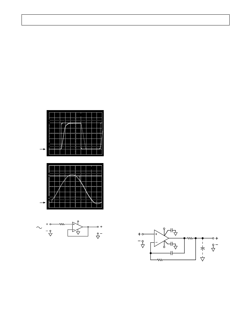
The AD824 does not exhibit phase reversal for input voltages up
to and including +V
S
. Figure 29a shows the response of an
AD824 voltage follower to a 0 V to +5 V (+V
S
) square wave in-
put. The input and output are superimposed. The output tracks
the input up to +V
S
without phase reversal. The reduced band-
width above a 4 V input causes the rounding of the output wave
form. For input voltages greater than +V
S
, a resistor in series
with the AD824’s noninverting input will prevent phase reversal
at the expense of greater input voltage noise. This is illustrated
in Figure 29b.
10
0%
100
90
1V
1V
10μs
1V
10
0%
100
90
1V
2μs
1V
GND
GND
+V
S
+5V
R
P
V
OUT
V
IN
Figure 29. (a) Response with R
P
= 0; V
IN
from 0 to +V
S
(b) V
IN
= 0 to + V
S
+ 200 m V
V
OUT
= 0 to + V
S
R
P
= 49.9 k
Since the input stage uses n-channel JFETs, input current dur-
ing normal operation is positive; the current flows out from the
input terminals. If the input voltage is driven more positive than
+V
S
– 0.4 V, the input current will reverse direction as internal
device junctions become forward biased. This is illustrated in
Figure 9.
(b)
(a)
相关PDF资料 |
PDF描述 |
|---|---|
| AD824AR-16 | VARISTOR 250V RMS 14MM RADIAL |
| AD824AR-3V | VARISTOR 35VRMS 14MM RADIAL |
| AD826 | High-Speed, Low-Power Dual Operational Amplifier |
| AD826 | Mini size of Discrete semiconductor elements |
| AD826AN | High-Speed, Low-Power Dual Operational Amplifier |
相关代理商/技术参数 |
参数描述 |
|---|---|
| AD824AR-14-3V-REEL | 功能描述:IC OPAMP JFET R-R 2MHZ LP 14SOIC RoHS:否 类别:集成电路 (IC) >> Linear - Amplifiers - Instrumentation 系列:- 标准包装:150 系列:- 放大器类型:音频 电路数:2 输出类型:- 转换速率:5 V/µs 增益带宽积:12MHz -3db带宽:- 电流 - 输入偏压:100nA 电压 - 输入偏移:500µV 电流 - 电源:6mA 电流 - 输出 / 通道:50mA 电压 - 电源,单路/双路(±):4 V ~ 32 V,±2 V ~ 16 V 工作温度:-40°C ~ 85°C 安装类型:表面贴装 封装/外壳:8-TSSOP(0.173",4.40mm 宽) 供应商设备封装:8-TSSOP 包装:管件 |
| AD824AR-14-REEL | 功能描述:IC OPAMP JFET R-R 2MHZ LP 14SOIC RoHS:否 类别:集成电路 (IC) >> Linear - Amplifiers - Instrumentation 系列:- 标准包装:150 系列:- 放大器类型:音频 电路数:2 输出类型:- 转换速率:5 V/µs 增益带宽积:12MHz -3db带宽:- 电流 - 输入偏压:100nA 电压 - 输入偏移:500µV 电流 - 电源:6mA 电流 - 输出 / 通道:50mA 电压 - 电源,单路/双路(±):4 V ~ 32 V,±2 V ~ 16 V 工作温度:-40°C ~ 85°C 安装类型:表面贴装 封装/外壳:8-TSSOP(0.173",4.40mm 宽) 供应商设备封装:8-TSSOP 包装:管件 |
| AD824AR-14-REEL7 | 功能描述:IC OPAMP JFET R-R 2MHZ LP 14SOIC RoHS:否 类别:集成电路 (IC) >> Linear - Amplifiers - Instrumentation 系列:- 标准包装:150 系列:- 放大器类型:音频 电路数:2 输出类型:- 转换速率:5 V/µs 增益带宽积:12MHz -3db带宽:- 电流 - 输入偏压:100nA 电压 - 输入偏移:500µV 电流 - 电源:6mA 电流 - 输出 / 通道:50mA 电压 - 电源,单路/双路(±):4 V ~ 32 V,±2 V ~ 16 V 工作温度:-40°C ~ 85°C 安装类型:表面贴装 封装/外壳:8-TSSOP(0.173",4.40mm 宽) 供应商设备封装:8-TSSOP 包装:管件 |
| AD824AR-16 | 制造商:Analog Devices 功能描述: 制造商:Rochester Electronics LLC 功能描述: 制造商:Analog Devices 功能描述:QUAD OP-AMP, 4000 uV OFFSET-MAX, 2 MHz BAND WIDTH, PDSO16 |
| AD824AR-16-REEL | 制造商:Analog Devices 功能描述:OP Amp Quad GP R-R O/P ±15V/30V 16-Pin SOIC N T/R |
发布紧急采购,3分钟左右您将得到回复。