- 您现在的位置:买卖IC网 > PDF目录16924 > AD8250-EVALZ (Analog Devices Inc)BOARD EVALUATION AD8250 PDF资料下载
参数资料
| 型号: | AD8250-EVALZ |
| 厂商: | Analog Devices Inc |
| 文件页数: | 21/24页 |
| 文件大小: | 0K |
| 描述: | BOARD EVALUATION AD8250 |
| 标准包装: | 1 |
| 系列: | iCMOS® |
| 每 IC 通道数: | 1 - 单 |
| 放大器类型: | 仪表 |
| 输出类型: | 单端 |
| 转换速率: | 25 V/µs |
| -3db带宽: | 10MHz |
| 电流 - 输出 / 通道: | 37mA |
| 工作温度: | -40°C ~ 85°C |
| 电流供应(主 IC): | 4.1mA |
| 电压 - 电源,单路/双路(±): | 10 V ~ 30 V,±5 V ~ 15 V |
| 板类型: | 完全填充 |
| 已供物品: | 板 |
| 已用 IC / 零件: | AD8250 |
| 相关产品: | AD8250ARMZ-R7DKR-ND - IC AMP INST ICMOS LDRIFT 10MSOP AD8250ARMZ-R7CT-ND - IC AMP INST ICMOS LDRIFT 10MSOP AD8250ARMZ-RL-ND - IC AMP INST ICMOS LDRIFT 10MSOP AD8250ARMZ-R7TR-ND - IC AMP INST ICMOS LDRIFT 10MSOP AD8250ARMZ-ND - IC AMP INST ICMOS LDRIFT 10MSOP |
AD8250
Data Sheet
Rev. C | Page 6 of 24
ABSOLUTE MAXIMUM RATINGS
Table 3.
Parameter
Rating
Supply Voltage
±17 V
Power Dissipation
Output Short-Circuit Current
Indefinite1
Common-Mode Input Voltage
+VS + 13 V, VS 13 V
Differential Input Voltage
Digital Logic Inputs
±VS
Storage Temperature Range
65°C to +125°C
Operating Temperature Range3
40°C to +85°C
Lead Temperature (Soldering, 10 sec)
300°C
Junction Temperature
140°C
θJA (Four-Layer JEDEC Standard Board)
112°C/W
Package Glass Transition Temperature
140°C
1
Assumes that the load is referenced to midsupply.
2
Current must be kept to less than 6 mA.
3
Temperature for specified performance is 40°C to +85°C. For performance
to 125°C, see the Typical Performance Characteristics section.
Stresses above those listed under Absolute Maximum Ratings
may cause permanent damage to the device. This is a stress
rating only; functional operation of the device at these or any
other conditions above those indicated in the operational section of
this specification is not implied. Exposure to absolute maximum
rating conditions for extended periods may affect device reliability.
MAXIMUM POWER DISSIPATION
The maximum safe power dissipation in the AD8250 package is
limited by the associated rise in junction temperature (TJ) on
the die. The plastic encapsulating the die locally reaches the
junction temperature. At approximately 140°C, which is the
glass transition temperature, the plastic changes its properties.
Even temporarily exceeding this temperature limit can change
the stresses that the package exerts on the die, permanently
shifting the parametric performance of the AD8250. Exceeding
a junction temperature of 140°C for an extended period can
result in changes in silicon devices, potentially causing failure.
The still-air thermal properties of the package and PCB (θJA),
the ambient temperature (TA), and the total power dissipated in
the package (PD) determine the junction temperature of the die.
The junction temperature is calculated as
TJ = TA + (PD × θJA)
The power dissipated in the package (PD) is the sum of the
quiescent power dissipation and the power dissipated in the
package due to the load drive for all outputs. The quiescent
power is the voltage between the supply pins (VS) times the
quiescent current (IS). Assuming that the load (RL) is referenced
to midsupply, the total drive power is VS/2 × IOUT, some of which
is dissipated in the package and some in the load (VOUT × IOUT).
The difference between the total drive power and the load
power is the drive power dissipated in the package.
PD = Quiescent Power + (Total Drive Power Load Power)
(
)
L
OUT
L
OUT
S
D
R
V
R
V
I
V
P
2
–
2
×
+
×
=
In single-supply operation with RL referenced to VS, the worst
case is VOUT = VS/2.
Airflow increases heat dissipation, effectively reducing θJA. In
addition, more metal directly in contact with the package leads
from metal traces, through holes, ground, and power planes
reduces the θJA.
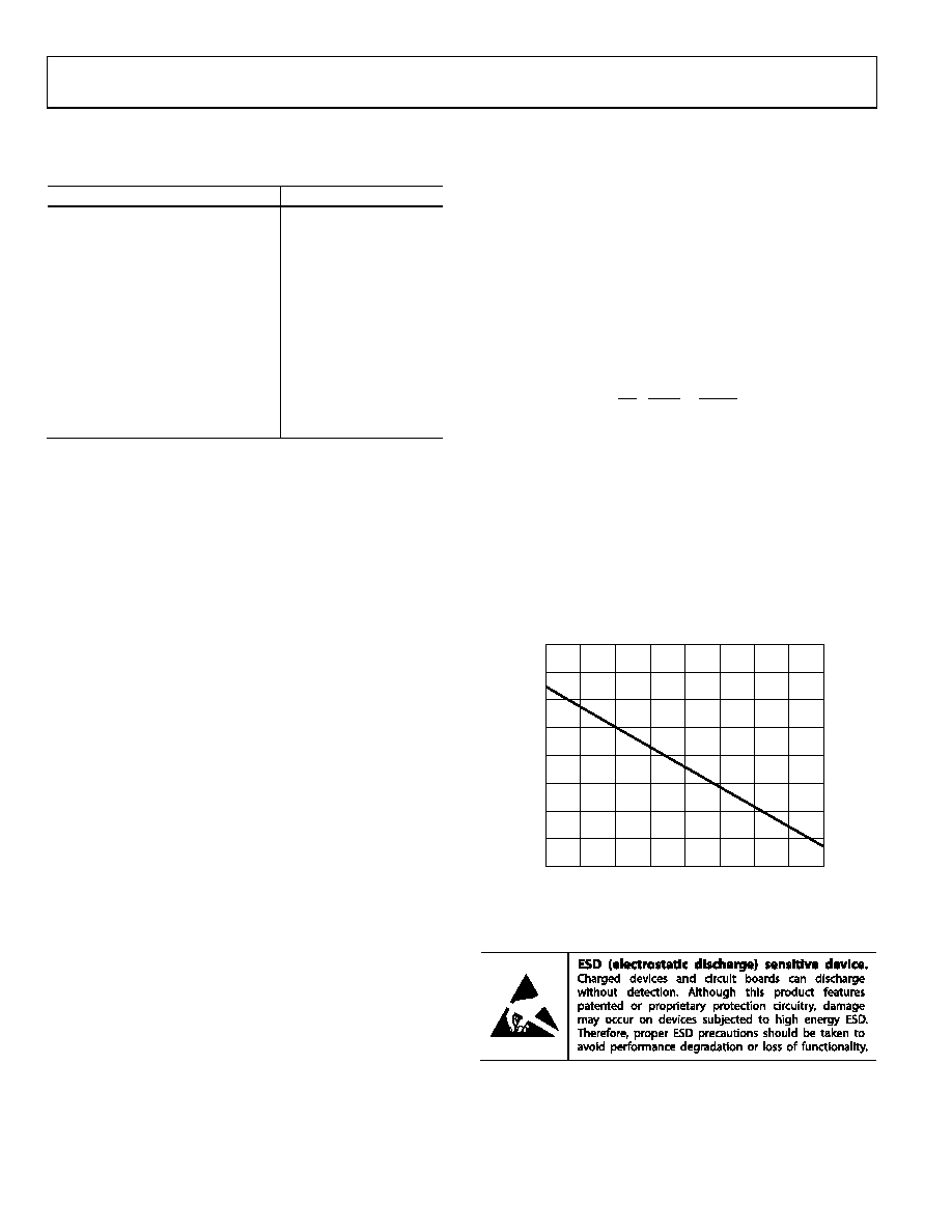
Figure 4 shows the maximum safe power dissipation in the
package vs. the ambient temperature on a four-layer JEDEC
standard board.
2.00
1.75
1.50
1.25
1.00
0.75
0.50
0.25
0
–40
–20
120
100
80
60
40
20
0
MA
XI
MU
M
PO
W
ER
D
ISSI
PA
T
IO
N
(W
)
AMBIENT TEMPERATURE (°C)
06288-
004
Figure 4. Maximum Power Dissipation vs. Ambient Temperature
ESD CAUTION
相关PDF资料 |
PDF描述 |
|---|---|
| 381LX221M400A012 | CAP ALUM 220UF 400V 20% SNAP |
| ISL60002BIH330Z-TK | IC VREF SERIES PREC 3V SOT-23-3 |
| 6-1589457-1 | WDUALOBE CONNECTOR |
| NCP571MN12TBGEVB | BOARD EVAL NCP571MN 1.2V |
| AD8310-EVALZ | BOARD EVAL FOR AD8310 |
相关代理商/技术参数 |
参数描述 |
|---|---|
| AD8251 | 制造商:AD 制造商全称:Analog Devices 功能描述:Wide Supply Range, Micropower, |
| AD8251_07 | 制造商:AD 制造商全称:Analog Devices 功能描述:10 MHz, 20 V/レs, G = 1, 2, 4, 8 i CMOS㈢ Programmable Gain Instrumentation Amplifier |
| AD8251ARMZ | 功能描述:IC AMP INST ICMOS LDRIFT 10MSOP RoHS:是 类别:集成电路 (IC) >> Linear - Amplifiers - Instrumentation 系列:iCMOS® 标准包装:1 系列:- 放大器类型:通用 电路数:4 输出类型:满摆幅 转换速率:0.028 V/µs 增益带宽积:105kHz -3db带宽:- 电流 - 输入偏压:3nA 电压 - 输入偏移:100µV 电流 - 电源:3.3µA 电流 - 输出 / 通道:12mA 电压 - 电源,单路/双路(±):2.7 V ~ 12 V,±1.35 V ~ 6 V 工作温度:-40°C ~ 85°C 安装类型:表面贴装 封装/外壳:14-TSSOP(0.173",4.40mm 宽) 供应商设备封装:14-TSSOP 包装:剪切带 (CT) 其它名称:OP481GRUZ-REELCT |
| AD8251ARMZ-R7 | 功能描述:IC AMP INST ICMOS LDRIFT 10MSOP RoHS:是 类别:集成电路 (IC) >> Linear - Amplifiers - Instrumentation 系列:iCMOS® 标准包装:2,500 系列:- 放大器类型:通用 电路数:4 输出类型:- 转换速率:0.6 V/µs 增益带宽积:1MHz -3db带宽:- 电流 - 输入偏压:45nA 电压 - 输入偏移:2000µV 电流 - 电源:1.4mA 电流 - 输出 / 通道:40mA 电压 - 电源,单路/双路(±):3 V ~ 32 V,±1.5 V ~ 16 V 工作温度:0°C ~ 70°C 安装类型:表面贴装 封装/外壳:14-TSSOP(0.173",4.40mm 宽) 供应商设备封装:14-TSSOP 包装:带卷 (TR) 其它名称:LM324ADTBR2G-NDLM324ADTBR2GOSTR |
| AD8251ARMZ-RL | 功能描述:IC AMP INST ICMOS LDRIFT 10MSOP RoHS:是 类别:集成电路 (IC) >> Linear - Amplifiers - Instrumentation 系列:iCMOS® 标准包装:150 系列:- 放大器类型:音频 电路数:2 输出类型:- 转换速率:5 V/µs 增益带宽积:12MHz -3db带宽:- 电流 - 输入偏压:100nA 电压 - 输入偏移:500µV 电流 - 电源:6mA 电流 - 输出 / 通道:50mA 电压 - 电源,单路/双路(±):4 V ~ 32 V,±2 V ~ 16 V 工作温度:-40°C ~ 85°C 安装类型:表面贴装 封装/外壳:8-TSSOP(0.173",4.40mm 宽) 供应商设备封装:8-TSSOP 包装:管件 |
发布紧急采购,3分钟左右您将得到回复。