- 您现在的位置:买卖IC网 > PDF目录373941 > AD826 (Analog Devices, Inc.) High-Speed, Low-Power Dual Operational Amplifier PDF资料下载
参数资料
| 型号: | AD826 |
| 厂商: | Analog Devices, Inc. |
| 英文描述: | High-Speed, Low-Power Dual Operational Amplifier |
| 中文描述: | 高速,低功耗双路运算放大器 |
| 文件页数: | 3/14页 |
| 文件大小: | 231K |
| 代理商: | AD826 |
REV. B
–3–
AD826
ABSOLUTE MAXIMUM RATINGS
1
Supply Voltage . . . . . . . . . . . . . . . . . . . . . . . . . . . . . . .
±
18 V
Internal Power Dissipation
2
Plastic (N) . . . . . . . . . . . . . . . . . . . . . See Derating Curves
Small Outline (R) . . . . . . . . . . . . . . . . See Derating Curves
Input Voltage (Common Mode) . . . . . . . . . . . . . . . . . . .
±
V
S
Differential Input Voltage . . . . . . . . . . . . . . . . . . . . . . .
±
6 V
Output Short Circuit Duration . . . . . . . See Derating Curves
Storage Temperature Range (N, R) . . . . . . . –65
°
C to +125
°
C
Operating Temperature Range . . . . . . . . . . –40
°
C to +85
°
C
Lead Temperature Range (Soldering 10 seconds) . . . +300
°
C
NOTES
1
Stresses above those listed under Absolute Maximum Ratings may cause perma-
nent damage to the device. This is a stress rating only; functional operation of the
device at these or any other conditions above those indicated in the operational
section of this specification is not implied. Exposure to absolute maximum rating
conditions for extended periods may affect device reliability .
2
Specification is for device in free air: 8-lead plastic package,
θ
JA
= 100
°
C/watt;
8-lead SOIC package,
θ
JA
= 155
°
C/watt.
ORDERING GUIDE
Temperature
Range
–40
°
C to +85
°
C 8-Lead Plastic DIP
–40
°
C to +85
°
C 8-Lead Plastic SOIC
AD826AR-REEL7 –40
°
C to +85
°
C 7” Tape & Reel SOIC
AD826AR-REEL
–40
°
C to +85
°
C 13” Tape & Reel SOIC SO-8
Package
Description
Package
Option
Model
AD826AN
AD826AR
N-8
SO-8
SO-8
Parameter
Conditions
V
S
Min
Typ
Max
Unit
OUTPUT CHARACTERISTICS
Output Voltage Swing
R
LOAD
= 500
R
LOAD
= 150
R
LOAD
= 1 k
R
LOAD
= 500
R
LOAD
= 500
±
5 V
±
5 V
±
15 V
±
15 V
0, +5 V
3.3
3.2
13.3
12.8
+1.5,
+3.5
50
50
30
3.8
3.6
13.7
13.4
±
V
±
V
±
V
±
V
V
mA
mA
mA
mA
Output Current
±
15 V
±
5 V
0, +5 V
±
15 V
Short-Circuit Current
Output Resistance
MATCHING CHARACTERISTICS
Dynamic
Crosstalk
Gain Flatness Match
Slew Rate Match
DC
Input Offset Voltage Match
Input Bias Current Match
Open-Loop Gain Match
90
8
Open Loop
f = 5 MHz
G = +1, f = 40 MHz
G = –1
±
15 V
±
15 V
±
15 V
–80
0.2
10
dB
dB
V/
μ
s
T
MIN
–T
MAX
T
MIN
–T
MAX
V
O
=
±
10 V, R
LOAD
= 1 k
,
T
MIN
–T
MAX
V
CM
=
±
12 V, T
MIN
–T
MAX
±
5 V to
±
15 V, T
MIN
–T
MAX
±
5 V to
±
15 V
±
5 V to
±
15 V
0.5
0.06
2
0.8
mV
μ
A
±
15 V
±
15 V
0.15
80
80
0.01
100
100
mV/V
dB
dB
Common-Mode Rejection Ratio Match
Power Supply Rejection Ratio Match
POWER SUPPLY
Operating Range
Dual Supply
Single Supply
±
2.5
+5
±
18
+36
7.5
7.5
7.5
7.5
V
V
mA
mA
mA
mA
dB
Quiescent Current/Amplifier
±
5 V
±
5 V
±
15 V
±
15 V
6.6
T
MIN
to T
MAX
T
MIN
to T
MAX
V
S
=
±
5 V to
±
15 V, T
MIN
to T
MAX
6.8
86
Power Supply Rejection Ratio
75
NOTES
1
Full power bandwidth = slew rate/2
π
V
PEAK
.
Specifications subject to change without notice.
ESD SUSCEPTIBILITY
ESD (electrostatic discharge) sensitive device. Electrostatic charges
as high as 4000 volts, which readily accumulate on the human
body and on test equipment, can discharge without detection.
Although the AD826 features proprietary ESD protection cir-
cuitry, permanent damage may still occur on these devices
if they are subjected to high energy electrostatic discharges.
Therefore, proper ESD precautions are recommended to avoid
any performance degradation or loss of functionality.
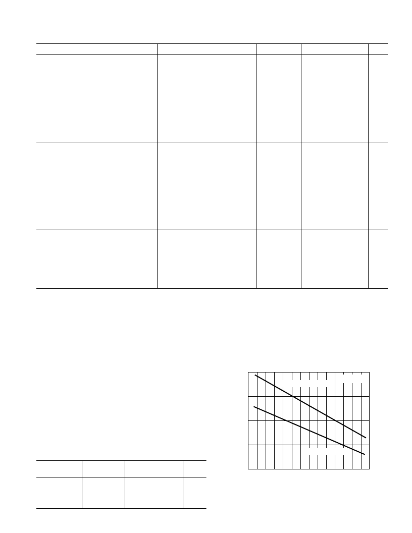
2.0
0
–
50
90
1.5
0.5
–
30
1.0
50
70
30
10
–
10
AMBIENT TEMPERATURE
–
C
80
–
40
40
60
20
0
–
20
M
–
8-LEAD MINI-DIP PACKAGE
8-LEAD SOIC PACKAGE
T
J
= +150 C
Maximum Power Dissipation vs. Temperature for Different
Package Types
相关PDF资料 |
PDF描述 |
|---|---|
| AD826 | Mini size of Discrete semiconductor elements |
| AD826AN | High-Speed, Low-Power Dual Operational Amplifier |
| AD826AR | High-Speed, Low-Power Dual Operational Amplifier |
| AD826AR-REEL | High-Speed, Low-Power Dual Operational Amplifier |
| AD826AR-REEL7 | High-Speed, Low-Power Dual Operational Amplifier |
相关代理商/技术参数 |
参数描述 |
|---|---|
| AD8260 | 制造商:AD 制造商全称:Analog Devices 功能描述:High Current Driver Amplifier and Digital VGA/Preamplifier with 3 dB Steps |
| AD8260ACPZ-R7 | 功能描述:IC AMP VGA DIFF LN 310MA 32LFCSP RoHS:是 类别:集成电路 (IC) >> Linear - Amplifiers - Instrumentation 系列:- 标准包装:50 系列:- 放大器类型:J-FET 电路数:2 输出类型:- 转换速率:13 V/µs 增益带宽积:3MHz -3db带宽:- 电流 - 输入偏压:65pA 电压 - 输入偏移:3000µV 电流 - 电源:1.4mA 电流 - 输出 / 通道:- 电压 - 电源,单路/双路(±):7 V ~ 36 V,±3.5 V ~ 18 V 工作温度:-40°C ~ 85°C 安装类型:通孔 封装/外壳:8-DIP(0.300",7.62mm) 供应商设备封装:8-PDIP 包装:管件 |
| AD8260ACPZ-RL | 功能描述:IC AMP VGA DIFF LN 310MA 32LFCSP RoHS:是 类别:集成电路 (IC) >> Linear - Amplifiers - Instrumentation 系列:- 标准包装:50 系列:- 放大器类型:J-FET 电路数:2 输出类型:- 转换速率:13 V/µs 增益带宽积:3MHz -3db带宽:- 电流 - 输入偏压:65pA 电压 - 输入偏移:3000µV 电流 - 电源:1.4mA 电流 - 输出 / 通道:- 电压 - 电源,单路/双路(±):7 V ~ 36 V,±3.5 V ~ 18 V 工作温度:-40°C ~ 85°C 安装类型:通孔 封装/外壳:8-DIP(0.300",7.62mm) 供应商设备封装:8-PDIP 包装:管件 |
| AD8260ACPZ-WP | 功能描述:IC AMP VGA DIFF LN 310MA 32LFCSP RoHS:是 类别:集成电路 (IC) >> Linear - Amplifiers - Instrumentation 系列:- 标准包装:2,500 系列:Excalibur™ 放大器类型:J-FET 电路数:1 输出类型:- 转换速率:45 V/µs 增益带宽积:10MHz -3db带宽:- 电流 - 输入偏压:20pA 电压 - 输入偏移:490µV 电流 - 电源:1.7mA 电流 - 输出 / 通道:48mA 电压 - 电源,单路/双路(±):4.5 V ~ 38 V,±2.25 V ~ 19 V 工作温度:-40°C ~ 85°C 安装类型:表面贴装 封装/外壳:8-SOIC(0.154",3.90mm 宽) 供应商设备封装:8-SOIC 包装:带卷 (TR) |
| AD8260-EVALZ | 功能描述:BOARD EVAL FOR AD8260 RoHS:是 类别:编程器,开发系统 >> 评估板 - 运算放大器 系列:- 产品培训模块:Lead (SnPb) Finish for COTS Obsolescence Mitigation Program 标准包装:1 系列:- |
发布紧急采购,3分钟左右您将得到回复。